Application Notes
Filter by:
Product Category
33
17
12
9
9
6
4
4
4
3
3
2
1
1
1
Application Notes
Optimization of Injection Molding Processes Using Design of Experiments
Application Note for MKS Instruments SenseLink™ QM for Optimization of Injection Molding Processes Using Design of Experiments
Application Notes
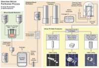
Silicon Wafer Production
The silicon wafers so familiar to those of us in the semiconductor industry are actually thin slices of a large single crystal of silicon that was grown from melted electronic grade …
Application Notes
Thin Film Deposition
The thin films that are used to fabricate microelectronic devices are all formed using some kind of deposition technology where the term refers to the formation of a deposit on a s …
Application Notes
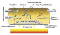
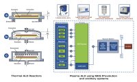
Low Pressure Chemical Vapor Deposition
Reactor configurations that have been used for LPCVD thin film processes include resistance heated tubular hot-wall reactors, vertical flow batch reactors and single-wafer reactors …
Application Notes
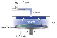
Plasma Enhanced Chemical Vapor Deposition
The key advantages sought in the use of PECVD vs. LPCVD were the ability to reduce process temperatures while maintaining or increasing deposition rates.
Application Notes
Atomic Layer Deposition
Atomic layer deposition is similar to LPCVD except that the chemical process is broken down into steps that isolate different adsorption and reaction steps to have self-limiting re …
Application Notes
Semiconductor Etching
Etching refers to any technology that will selectively remove material from a thin film on a substrate and by this removal create a pattern of that material on the substrate.
Application Notes
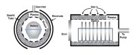
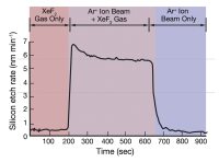
Isotropic Radical Etching
High pressure plasma etching processes typically operate around 0.2 - 2 Torr. These are glow discharge methods that etch material via a chemical rather than a physical mechanism.
Application Notes
Reactive Ion Etching
Reactive Ion Etching (RIE) uses a combination of chemical and physical reactions to remove material from a substrate; it is the simplest process that is capable of directional etch …
Application Notes
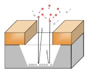
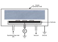
Physical Sputtering and Ion Milling
Sputtering and ion milling are purely physical processes in which heavy atomic positive ions, created in a plasma, are accelerated to impact a substrate surface to remove material.
Application Notes
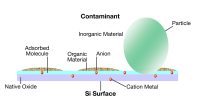
Wafer Surface Cleaning
Prior to a wafer's entry into the fabrication process, its surface must be cleaned to remove any adhering particles and organic/inorganic impurities. Silicon native oxide also needs …
Application Notes
Wet Substrate Surface Cleaning
This note describes some of the equipment used for wet cleaning silicon substrates in modern semiconductor fabrication plants from very simple "wet bench" cleaning stations to sophisticated …
Application Notes
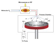
Dry Substrate Surface Cleaning
Photoresist stripping involves the removal of photoresist residues by reaction with atomic oxygen radicals or some other highly reactive species to produce a volatile product that can …
Application Notes
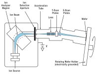
Ion Implantation
Ion implantation owes its importance to the fact that it allows precise control over the depth of penetration of dopant atoms into the silicon. In the ion implantation process, dopant …
Application Notes
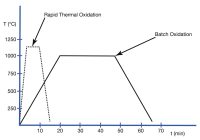
Thermal Oxidation
Thermal oxides are used primarily for gate oxides in silicon semiconductor devices. It is critical that the silicon dioxide interface be as perfect as possible with a minimum of atomic …
Application Notes
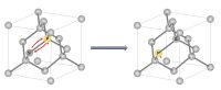
Dopant Atom Diffusion
Diffusion can be described as a "smoothing out" of any localized high concentration of impurity atoms that is driven by the motion of the atoms in the material and by their mobility …

Application Notes
Thermal Annealing
Conventional, high-temperature annealing is used in device manufacturing to relieve stress in silicon; to activate ion-implanted dopants and to reduce structural defects and stress; …
Application Notes
CMOS Wafer Processing
The initial step in the CMOS process is the formation of a "pad" thermal silicon dioxide layer on the wafer surface. The pad oxide relieves stress between the substrate and the subsequent …

Application Notes
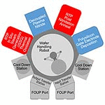
Baratron® Capacitance Manometer Selection and Installation
Appropriate design techniques be used for the selection and installation of Baratron® Capacitance Manometers
 Ultra-High Velocity