Thin Film Deposition
The thin films that are used to fabricate microelectronic devices are all formed using some kind of deposition technology where the term refers to the formation of a deposit on a substrate. In semiconductor device manufacture the following deposition technologies (along with their commonly used acronyms) are:
- Low Pressure Chemical Vapor Deposition - LPCVD
- Plasma Enhanced Chemical Vapor Deposition - PECVD
- Sub-Atmospheric Pressure Chemical Vapor Deposition - SACVD
- Atmospheric Pressure Chemical Vapor Deposition - APCVD
- Atomic Layer Deposition - ALD
- Physical Vapor Deposition - PVD
- Ultra-High Vacuum Chemical Vapor Deposition - UHV-CVD
- Diamond-Like Carbon - DLC
- Commercial Film - C-F
- Epitaxial Deposition - Epi
Chemical Vapor Deposition and Thin Film Formation
Chemical vapor deposition processes can be defined as any process in which a thin solid film is formed on a substrate by the surface-mediated reaction of adsorbed precursors from the gas phase. The reactive nature of CVD processes distinguishes them from physical processes such as evaporation and sputtering that are employed in PVD. The term "surface-mediated" refers to the fact that the solid film is formed by a heterogeneous reaction occurring at the substrate surface. See Chemical Vapor Deposition Physics for additional information.
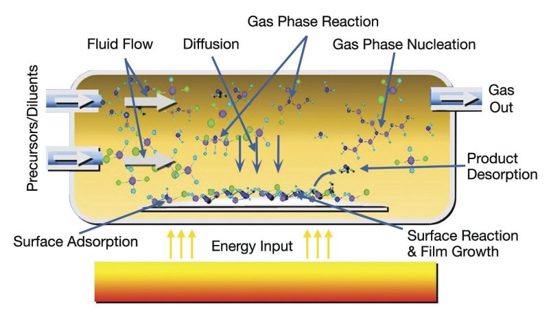
Figure 1. Aspects of a CVD process.
Figure 1 shows a schematic that can help in understanding the different processes in a CVD reactor. Chemical vapor deposition processes can be broken down into a number of discrete steps: First the precursor chemicals must be fed into the CVD reactor. Once in the reactor, precursor molecules must be transported to the substrate surface, usually through a combination of fluid transport and diffusion. Once on the surface, the precursor molecule must remain there long enough to react. After reaction occurs, the product thin film atom must remain on the surface while the by-product molecules must desorb from the substrate surface to make room for more incoming precursor molecules.
Typical CVD Process Thin Films
Typical films produced by CVD processes include:
- Epitaxial Silicon
- Epitaxial Compound Semiconductors
- Polycrystalline Silicon
-
Dielectric Thin Films
- Silicon Dioxide (including P- and B-doped Oxides)
- Aluminum Oxide
- Low-k Dielectrics (SiO-F, DLC, amorphous C-F)
- Silicon Nitride
- Titanium Nitride
- Tantalum Nitride
- Transition Metal Oxides (i.e. TiO2, ZrO2, Hf2O5, Ta2O5)
- Metals (Al, W, Cu)
- Silicides (WSix, CoSix)
Low Pressure Chemical Vapor Deposition (LPCVD)
LPCVD deposition systems typically operate at pressures that range from 0.1 to 10 Torr. Reactor configurations that have been used for LPCVD thin film processes include resistance heated tubular hot-wall reactors, vertical flow batch reactors and single-wafer reactors. Modern fabs have largely migrated to the use of single wafer cluster tools for CVD and other processing needs owing to demonstrated advantages in wafer handling, effective particle and process control and process integration. See Low Pressure Chemical Vapor Deposition Systems for additional information.
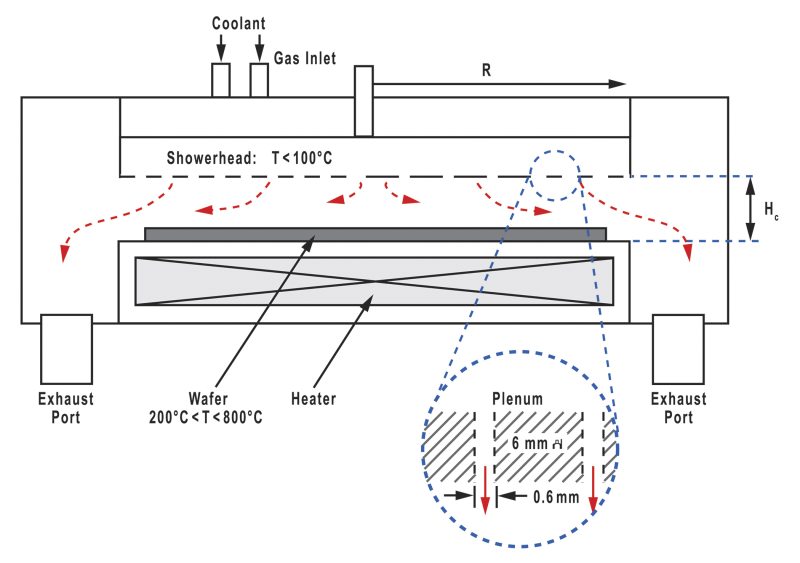
Figure 2. A typical single wafer CVD process chamber configuration.
Plasma Enhanced Chemical Vapor Deposition (PECVD)
Plasma enhanced CVD systems, like LPCVD systems, began as batch processors for loads of up to 100 wafers at a time. The key advantages sought in the use of PECVD vs. LPCVD were the ability to reduce process temperatures while maintaining or increasing deposition rates. As device geometries grew ever smaller, limiting time-at-temperature became more important in maintaining the material properties and electrical characteristics of the components already in place on partially fabricated devices. As PECVD processes matured, other advantages such as the ability to manipulate thin film material and conformational properties became apparent. The early commercial configurations for PECVD processing were derived from LPCVD technology of the time, with the PECVD process performed in an evacuated (2-10 Torr) hot-wall tube reactor environment (Figure 3). See Plasma Enhanced Chemical Vapor Deposition Systems for additional information.
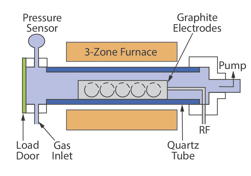
Figure 3. A typical single wafer CVD process chamber configuration.
Sub-Atmospheric Pressure Chemical Vapor Deposition (SACVD)
The primary application for SACVD equipment is in the TEOS/ozone silicon dioxide CVD process. TEOS/O3 processes fulfill the need for reduced time-at-temperature in interlevel dielectric processing for ULSI. Additionally, TEOS/O3 has self-planarizing characteristics superior to other silicon dioxide thin film deposition process.
Atomic Layer Deposition (ALD)
Atomic layer deposition is similar to LPCVD except that the chemical process is broken down into steps that isolate different adsorption and reaction steps to have self-limiting reactions. The process employs separate pulses of precursors and reactants that pass sequentially through the process chamber. Figure 4 illustrates the ALD process. With the substrate in the process chamber and under high vacuum, an initial precursor is introduced into the chamber. The molecular character of the precursor is such that it will form a chemically-bound monolayer on the substrate surface (Step 1). Any layers beyond the monolayer are only bound by physisorption forces which are weak enough to allow any precursor other than that in the monolayer to be pumped away under high vacuum. Once the monolayer is present on the substrate, the chamber is re-evacuated and purged to remove any excess precursor (Step 2). Next, a reactant is introduced to the process chamber (Step 3). It reacts with the monolayer material to form the desired compound on the substrate surface (Step 4). By-products of this reaction are pumped away. See Atomic Layer Deposition for additional information.
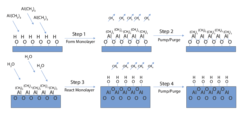
Figure 4. A typical single wafer CVD process chamber configuration.
Physical Vapor Deposition (PVD)
Physical Vapor Deposition (PVD) processes deposit thin films by using physical processes such as evaporation or sputtering. These processes vaporize material from a solid source under high temperature/high vacuum or plasma and redeposit the material on the substrate surface. Thermal evaporation and sputtering are the primary methods of PVD. Thermal evaporation vaporizes the source material by heating it in vacuum while sputtering uses a plasma to produce ion bombardment (normally argon ions) that creates a vapor from the source material. Films that can be deposited by PVD include most metals and dielectric materials.
Thin Film Deposition Products
Precursor Delivery Products (except ALD)
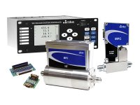
Thermal and pressure-based Mass Flow Controllers (MFCs) and Meters (MFMs) are designed to meet a broad variety of processing applications. Most MKS mass flow control and metering products offer both analog (0-5 VDC; 4-20 mA) and digital (Devicenet, Profibus, EtherCAT, RS485) I/O with embedded Modbus and an Ethernet user interface.
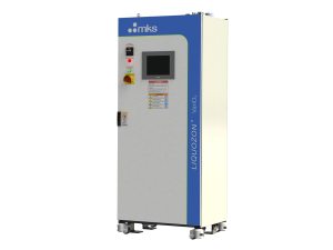
Ozone gas delivery products are suitable for a variety of purposes including TEOS/O3 SACVD. They incorporate field proven, high concentration, ultra-clean ozone generation technology as well as integrated ozone concentration monitor, flow control, and power distribution. Safety monitors, status indicator, and ozone destruct are available on some models.
Flow Ratio Control Products
MKS offers a line of digitally controlled, web-enabled gas flow ratio measurement and control technology for multi-channel gas flow distribution. The DELTA™ II mass flow ratio controller divides and controls mixed process gas flows to either multiple chambers or zones within a process chamber at ratios specified by the user to maximize process uniformity and repeatability. The DELTA II is used in a variety of flow splitting applications, including etch, strip and CVD.
Plasma Generator Products (PECVD)
RF Power Generators deliver reliable solid state power for today's thin film deposition applications. MKS RF generators insure consistent, repeatable power delivery in the most critical applications.
The SurePower 13.56 MHz product line offers the highest power density available, up to 13 kW in a 3U full rack package. SurePower uses patented intrinsic power amplifier protection and embedded V-I sensor to achieve superior reliability and power accuracy.
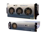
The KEINOS™ line of plasma generators are designed for pulsed duty applications in environments that experience fast impedance changes such as PECVD. The KEINOS line of generators delivers up to 13 kW of power with pulsing to 20 KHz, multiple set point pulsing, pulse shaping, and frequency tuning. MKS also produces a line of pulsed DC power generators for use in PECVD applications.
Reactive Gas Generators
MKS offers a variety of plasma-based reactive gas generators designed for both general use and for specific processes. These generators provide reliable sources of active NF3 and other fluorine-based radical species as well as reactive species derived from O2, N2, H2 and H2O. These generators find application in deposition technologies in which remote sources of plasma species are needed and in maintenance functions such as the generation of reactive species for CVD chamber cleaning.
The AX7610 is a general duty microwave plasma source for use in remote plasma applications and reactive gas generation. It is designed to be integrated into a microwave plasma subsystem comprised of power supplies, microwave magnetron heads, matching systems, etc. MKS offers a variety of microwave power generators, magnetron heads and system accessories.
Plasma Sources for PVD Thin Film Deposition Reactors
MKS offers a line of RF and DC power generators for applications that include PVD and direct plasma PECVD applications. Product frequencies range from DC to high RF frequencies with power levels up to 100 kW.
Products for ALD Systems
MKS offers the high performance P-Series MFCs and meters for applications in ALD processing. These are metal sealed, pressure insensitive MFC/MFMs with full scales up to 250 slm. Key for precise gas pulse production in ALD applications, they exhibit less than 750 millisecond settling time and are multi-gas, multi-range units with both analog and digital I/O and embedded Modbus and Ethernet user interfaces.
Ozone generation products from MKS are suitable for a variety of purposes including TEOS/O3 SACVD. They incorporate field proven, high concentration, ultra-clean ozone generation technology as well as integrated ozone concentration monitor, flow control, and power distribution. Safety monitors, status indicator, and ozone destruct are available on some models.
The Paragon H* and R*evolution remote plasma sources find use in ALD as an ultra-clean source of reactive gas for wafer pre-cleaning to promote film adhesion as well as for generating reactive precursors.
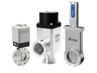
The T3Bi exhaust throttle valve, an intelligent, high speed exhaust valve, provides fast downstream vacuum/pressure control for ALD applications. This throttle valve is designed for fast recovery from flow and pressure variations, a pre-requisite for vacuum control in ALD systems.
Gas Composition and Process Monitors (CVD, ALD, PVD)
MKS gas composition monitors are based on Fourier-transform infrared spectroscopy (FTIR) and quadrupole mass spectrometer (QMS) technologies. The MultiGas™ 2030 is an operator-friendly FTIR-based analyzer capable of ppb to ppm sensitivity for multiple gas species process monitoring applications. It has permanently stored calibration spectra, simplifying installation and calibration needs. The Vision 2000-C™ gas analyzer is an application-specific RGA designed for continuous in situ monitoring of chemical vapor deposition (CVD) and etching processes during chamber clean, passivation and deposition. The Vision 2000-C is designed to detect subtle changes in low concentration species and high mass species decay with respect to time.
MKS also offers the Process Sense™ non-dispersive infrared (NDIR) analyzer for use in monitoring CVD and etch chamber cleaning processes. The Process Sense™ endpoint sensor is a small, low cost partial-pressure analyzer specifically designed to determine the completion of plasma chamber cleaning of deposition chambers. Process SenseÊis based on near infrared absorption.
Effluent Management Systems
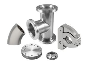
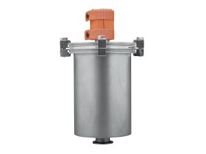
Downstream effluents in some thin film manufacturing processes can lead to yield loss and excessive equipment downtime due to clogged forelines, damaged pumps and valves, and contaminated transducers. Clogged lines simultaneously reduce flow conductance and raise particle counts. Effluent problems can also create serious safety issues. MKS has developed a series of process traps and effluent management solutions and vacuum line heaters to help maintain clear piping.
Automation and Control Systems
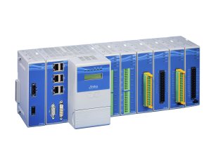
MKS offers a Programmable Automation Platform (PAC) that can be easily configured to perform standard control and automation tasks. The advanced analytics feature of the Automation Platform provides a smarter automation solution. It can be configured to connect, monitor, control, analyze, and optimize processes, fully delivering on the concept of "learned" automation. The Automation Platform supports the MKS SenseLink™ QM application for real-time multivariate analytics, incorporates knowledge and solutions in design of experiments (DOE) and process optimization, and applies it to controls and automation. In addition to supporting advanced control algorithms (both MKS and third party), the Automation Platform easily integrates with other MKS devices and instruments including pressure gauges, mass flow controllers, valves, gas analysis solutions, etc.
Pressure Measurement
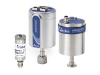
Baratron capacitance manometers are widely used for direct pressure measurement in thin film deposition applications.
Related Topics
Thin Films
- Polycrystalline Silicon Thin Films
- Silicon Based Epitaxial Thin Films
- Compund Semiconductor Epitaxial Thin Films
- Dielectric Thin Films
- Metal Thin Films
Thin Film Deposition
For additional insights into semiconductor topics like this, download our free MKS Instruments Handbook: Semiconductor Devices & Process Technology
Request a Handbook Ultra-High Velocity