Semiconductor Etching
Figure 1. Etching to create a pattern on a substrate.
In semiconductor device fabrication, etching refers to any technology that will selectively remove material from a thin film on a substrate (with or without prior structures on its surface) and by this removal create a pattern of that material on the substrate. The pattern is defined by a mask that is resistant to the etching process, the creation of which was described in detail in Photolithography. Once the mask is in place, etching of the material that is not protected by the mask can occur, by either wet chemical or by "dry" physical methods. Figure 1 shows a schematic representation of this process.
Historically, wet chemical methods played a significant role in etching for pattern definition, up until the advent of VLSI and ULSI technology. However, as device feature sizes were reduced and surface topographies grew more critical, wet chemical etching gave way to dry etching technologies. This shift was due, primarily, to the isotropic nature of wet etching. Wet etching produces material removal in all directions, as shown in Figure 2, which results in a discrepancy between the feature size defined by the mask and that which is replicated on the substrate. VLSI and ULSI designs demand much more precise mask to pattern feature size correlation than was needed at larger feature sizes. In addition, aspect ratios (depth to width ratios) in advanced devices increased and achieving these ratios required an ability to anisotropically etch material using directional etching technologies. Figure 3 provides a schematic to help in understanding isotropic vs. anisotropic feature generation and directional etching. The final blow to wet etching's utility in advanced processing may have been the fact that many of the newer materials being used for device fabrication did not have accessible wet chemistries that could be employed for etching. These issues combined to relegate wet etch technologies to nearly exclusive use for cleaning rather than in etching applications. Only devices that have relatively large feature sizes (such as some MEMS structures) continue to employ wet methods for etching. Surface cleaning has been discussed in detail in Wafer Surface Cleaning.
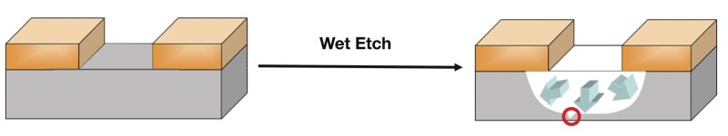
Figure 2. The isotropic character of wet etch processes.
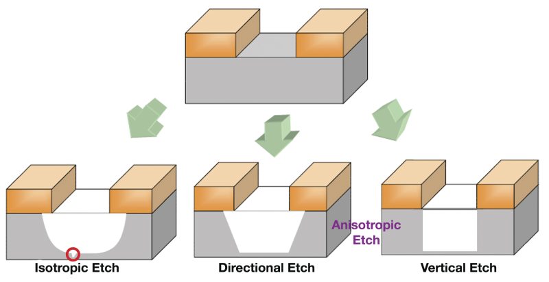
Figure 3. The isotropic character of wet etch processes.
Anisotropic etching uses a suite of technologies cumulatively known as "dry" etch. These technologies are universally used for etching in VLSI and ULSI device fabrication and they will be the only methods discussed in detail in this Section. Dry etching can remove material through physical means such as ion impact accompanied by ejection of material from the substrate or by chemical reactions that convert substrate material to volatile reaction products that can be pumped away. Dry etching technologies include the following commonly used methods (whether the etch process occurs through chemical etching, physical etching, or a combination as noted in parenthesis):
- Isotropic Radial Etching (Chemical)
- Reactive Ion Etching (Chemical/Physical)
- Sputter Etching (Physical)
- Ion Milling (Physical)
- Ion Beam Assisted Etching (Physical)
- Reactive Ion Beam Etching (Chemical/Physical)
All dry etching technologies are conducted under vacuum conditions with the pressure dictating, to some extent, the nature of the etch phenomenon.
Table 1 is taken from Wolf and Tauber and shows the relative pressure regime and generalized characteristics for the different etch methods. While there are a number of specific variants on the equipment and process characteristics used for etching, we will limit our discussion to a brief description of the process basics and the three primary etching methodologies identified in Table 1.
| Physical Sputtering and Ion Beam Milling | ||
| < 100 m Torr |
|
Higher Excitation Energy |
| Reactive Ion Etch | ||
| ~ 100 mTorr |
|
|
| Isotropic Radial Etching | ||
| Higher Pressure |
|
Lower Excitation Energy |
Table 1. Pressure regimes and characteristics for different etch methods.
Basic Processes
In-depth discussions of plasma etching fundamentals are available in a number of texts (Wolf and Tauber, Sze) and the interested reader is referred to these sources. Here we provide only the briefest description of the basic fundamentals of plasma generation. Within a plasma etching process, a number of physical phenomena are at work. When a strong electrical field is created in a plasma chamber using either electrodes (in the case of a DC potential or RF excitation) or a waveguide (in the case of microwaves), the field accelerates any available free electrons raising their internal energy (there are always a few free electrons in any environment resulting from cosmic rays, etc.). Free electrons collide with atoms or molecules in the gas phase and, if the electron transfers enough energy to the atom/molecule in the collision, an ionization event will occur producing a positive ion and another free electron. Collisions that transfer insufficient energy for ionization can nevertheless transfer sufficient energy to create a stable but reactive neutral species (i.e., molecular radicals). When sufficient energy is fed to the system, a stable, gas-phase plasma containing free electrons, positive ions and reactive neutrals is produced.
In plasma etching processes, the atomic and molecular ions and/or reactive neutrals from a plasma can be used to remove material from the substrate by either physical or chemical pathways, or by mechanisms that employ both. Purely physical etching (Figure 4) is accomplished by using strong electric fields to accelerate positive atomic ions (usually an ion of a heavy inert element such as argon) towards the substrate. This acceleration imparts energy to the ions and when they impact the substrate surface, their internal energy is transferred to the atoms in the substrate. If sufficient energy is transferred, a substrate atom will be ejected into the gas phase to be pumped away by the vacuum system. The incident ion is neutralized in the collision and, since it is a gas, it desorbs into the gas phase to be re-ionized or pumped out of the system.
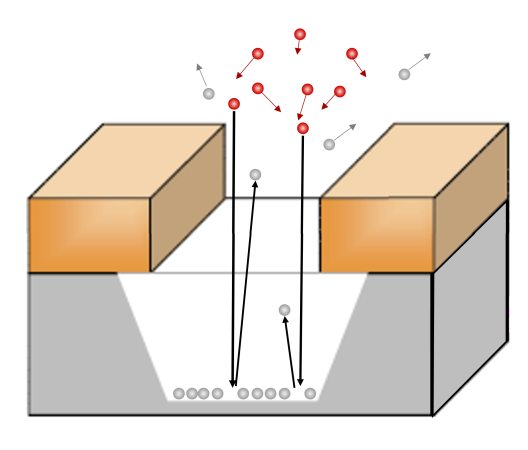
Figure 4. Physical etching of a substrate.
Chemical etching differs from physical etching in that it employs a chemical reaction between reactive neutral species created within the plasma and the substrate material. The most common type of chemical etching involves halide chemistries in which chlorine or fluorine atoms are the active agent in the etching process. A representative chemistry for etch processes is the use of NF3 for silicon etching. The chemical reaction sequence in this etch process is:
NF3 + e- → •NF2 + F• + e-
Si(s) +4F• → SiF4↑
NF3 is dissociated in the plasma to produce highly reactive atomic fluorine radicals. These radicals react with silicon in the substrate to produce silicon tetrafluoride, SiF4, which is a volatile gas that can be pumped away. In this manner silicon is etched from the substrate. Chemical etching, like wet etching, is an isotropic process without directionality (Figure 5). The reason for this is that the sticking coefficient of reactive neutrals is relatively low, so most impacts with the substrate surface do not result in etching, but rather with simple desorption of the reactive neutral back into the gas phase. This phenomenon results in an evening-out of the etch process within the feature being etched and ultimately isotropic character in the etch.
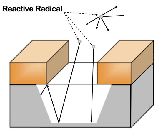
Figure 5. The source of isotropic character in plasma etching.
Most of the etching technologies used in modern device fabrication incorporate aspects of both physical and chemical etching. In processes such as reactive ion etching (RIE), directional etching is achieved by biasing the substrate so that ionic species from the plasma are accelerated towards the substrate surface. There they interact with the surface and the reactive neutrals to produce volatile products that can be pumped away (Figure 6). The ion energy in RIE is much lower than that employed for physical etching technologies and ion bombardment effects are negligible. The transfer of ion energies to the surface can enhance the directionality through improved adsorption of reactant species on the bombarded surface (incoming ions create high energy defects where adsorption and reaction preferentially occur) and through enhanced by-product desorption (incoming ion energies are transferred to reaction products causing them to desorb from the surface).
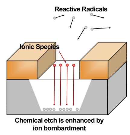
Figure 6. Chemical etch enhanced by low energy ion bombardment.
Semiconductor Etching Products


Related Topics
Semiconductor Etching
Front-end Semiconductor
For additional insights into semiconductor topics like this, download our free MKS Instruments Handbook: Semiconductor Devices & Process Technology
Request a Handbook Ultra-High Velocity