Physical Sputtering and Ion Milling
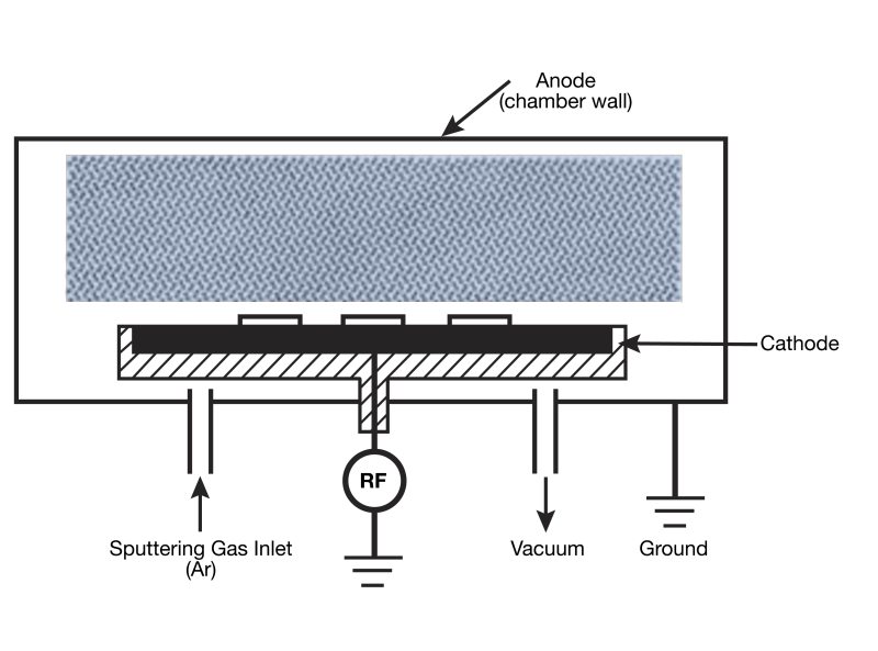
Figure 1. Physical sputter etch tool configuration.
Sputtering (Figure 1) and ion milling (Figure 2) are purely physical processes in which heavy atomic positive ions, created in a plasma, are accelerated to impact a substrate surface to remove material. The ion energies in these processes are high, often greater than 500 eV. Their primary advantage is the fact that they are highly anisotropic processes, producing features with near perfect vertical character. On the negative side, these processes are not particularly selective, having a tendency to etch all materials on the surface. Surface damage is also a problem in these processes. The etch rates that are achievable using physical sputtering are quite low when compared with chemical methods such as plasma etch and RIE. Ion milling is a method that has been developed to increase the etch rate in these processes. In ion milling, heavy ions (Ar+) are generated in a plasma confined to a discharge chamber separate from the process chamber. A negatively biased grid accelerates the ions out of the discharge chamber to form an ion beam in the process chamber. The process chamber is maintained under high vacuum (10-6 Torr) to maintain the coherence of the ion beam until it strikes the mounted substrate. In general, these processes are not widely used in advanced device fabrication. Figure 194 shows a schematic of an ion milling etch system.
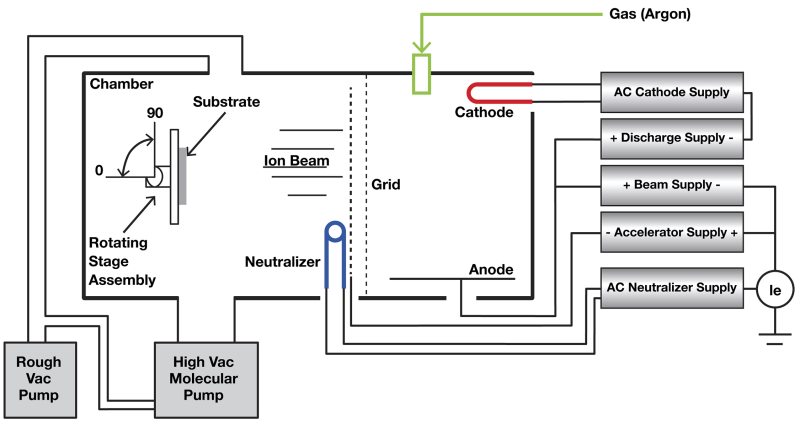
Figure 2. Ion beam etch system.(Used with permission from Microfab Inc.).
Related Topics
Semiconductor Etching
For additional insights into semiconductor topics like this, download our free MKS Instruments Handbook: Semiconductor Devices & Process Technology
Request a Handbook Ultra-High Velocity