Electrical Conduction in Solids
The physical mechanism of electrical conduction in solids is best understood using a model that physicists refer to as "band theory", which is based on the idea that the state of an electron in a solid is described by a four-fold scheme of quantum numbers. A useful analogy for electrons in a solid is that of spectators in an amphitheater. The electrons can be considered as spectators sitting in the amphitheater and the quantum numbers describe how many rows and seats are available. The energy state of individual electrons is described by a combination of four quantum numbers; this can be considered as analogous to the position of a spectator in an amphitheater which is described by a particular row and seat. Like spectators in an amphitheater moving between seats and rows, electrons can change their status, provided that there are spaces available for them to move into and provided that they have sufficient energy to make the move. If an electron (spectator) is to move into a higher-energy electron shell (higher row seat), it requires that additional energy to be given to the electron from an external source to move it further out in the electrical potential of the atom's nucleus. Using the amphitheater analogy, it takes an increase in energy (i.e., work) for a person to move into a higher row of seats, because that person must climb to a greater height against the force of gravity. Conversely, an electron "leaping" into a lower shell gives up some of its energy, like a person jumping down into a lower row of seats.
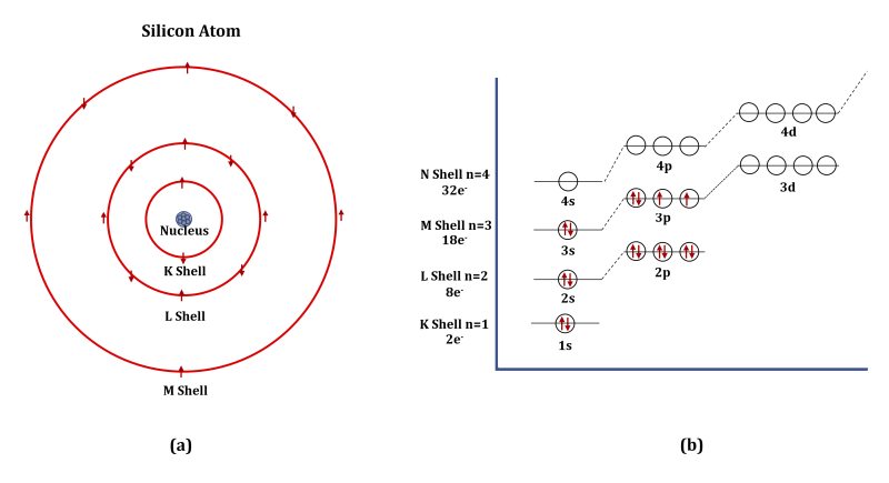
Figure 1. The silicon atom, showing (a) electron orbitals and (b) relative orbital energies.
In band theory, the electrons in a solid exist within "energy bands" (using our amphitheater analogy, energy bands can be viewed as seating sections containing many rows with equal quality seating). The model for the manner by which energy bands arise in a solid is most easily understood by first considering the energy of electrons in a single atom. Figure 1(a), shows a Bohr depiction of a single silicon atom. In this model of the atom, electrons occupy discrete orbitals or "shells" around the central atomic nucleus and each shell has a characteristic energy. For the silicon atom depicted in Figure 1(a), the atom's 14 electrons occupy three shells. The shells in (a) are designated, proceeding from the inside out, as K, L and M (there are higher shells, designated N, O, P, etc. in larger atoms). Different shells hold different numbers of electrons: the K shell holds two electrons; the L shell holds eight electrons; and the M shell holds 18 electrons (the N shell holds 32). In the very simplistic terms of the Bohr model of the atom, the number of electrons that a shell can hold correlates, very roughly, with the available surface area of the sphere defined by that shell, as one might expect from simple considerations of the repulsive forces atoms. In isolated atoms, the electrons exist in discrete electron orbital shells (labelled s and p in Figure 1). The energy gap between particles having the same charge (modern models of atomic structure are much more complex than this simple view).
Within each of the electron shells of an atom, electrons can occupy sub-shells of varying energy; these are designated by the letter s, p, d or f. Figure 1(b) shows these sub-shells represented as circles and the relative energies and ordering of the shells and sub-shells. Each sub-shell (circle) can hold a maximum of two electrons. The smallest K shell is only big enough to accommodate a single s sub-shell and therefore contains a maximum of two electrons. The larger L shell can accommodate one s sub-shell and three higher energy p sub-shells. Each p sub-shell is iso-energetic with the other two but is differentiated from its two partners by quantum numbers that we will not consider in this simplified discussion. The availability of s and p sub-shells allows the L shell to hold up to 8 electrons. The M shell includes one s sub-shell, three p sub-shells and five d sub-shells (as with the p sub-shells, the five d sub-shells are iso-energetic) and accommodates up to 18 electrons; higher energy shells hold correspondingly greater numbers of electrons. When the available sub-shells within a shell are all filled by electrons, then that shell is said to be "closed" and the electrons within that shell are no longer available for chemical interactions or electrical conduction. Silicon, shown in Figure 1(a), has 14 electrons. These electrons are sequentially accommodated in the available shells, starting at the lowest energy K shell. For silicon, the K and L shells are completely filled (10 electrons) and the M shell is unfilled, with only four electrons occupying the available nine sub-shells (the nine sub-shells can accommodate up to 18 electrons); these electrons are distributed in the lower energy s and p sub-shells. These four electrons in the outer or highest energy electron shell, are commonly termed the "valence" electrons; they determine silicon's chemical and electrical properties. An alternate way of depicting the energy shells and sub-shells in the silicon atom and the way that the sub-shells are filled is shown in Figure 2. Figure 2 clearly shows the "closed" shell core electrons in the silicon K and L shells and the valence electrons in the unfilled M shell.

Figure 2. Relative electron energy levels and ub-shell filling pattern for the silicon atom.
Within each of the electron shells of an atom, electrons can occupy sub-shells of varying energy; these are designated by the letter s, p, d or f. Figure 1(b) shows these sub-shells represented as circles and the relative energies and ordering of the shells and sub-shells. Each sub-shell (circle) can hold a maximum of two electrons. The smallest K shell is only big enough to accommodate a single s sub-shell and therefore contains a maximum of two electrons. The larger L shell can accommodate one s sub-shell and three higher energy p sub-shells. Each p sub-shell is iso-energetic with the other two but is differentiated from its two partners by quantum numbers that we will not consider in this simplified discussion. The availability of s and p sub-shells allows the L shell to hold up to 8 electrons. The M shell includes one s sub-shell, three p sub-shells and five d sub-shells (as with the p sub-shells, the five d sub-shells are iso-energetic) and accommodates up to 18 electrons; higher energy shells hold correspondingly greater numbers of electrons. When the available sub-shells within a shell are all filled by electrons, then that shell is said to be ÒclosedÓ and the electrons within that shell are no longer available for chemical interactions or electrical conduction. Silicon, shown in Figure 1(a), has 14 electrons. These electrons are sequentially accommodated in the available shells, starting at the lowest energy K shell. For silicon, the K and L shells are completely filled (10 electrons) and the M shell is unfilled, with only four electrons occupying the available nine sub-shells (the nine sub-shells can accommodate up to 18 electrons); these electrons are distributed in the lower energy s and p sub-shells. These four electrons in the outer or highest energy electron shell, are commonly termed the "valence" electrons; they determine silicon's chemical and electrical properties. An alternate way of depicting the energy shells and sub-shells in the silicon atom and the way that the sub-shells are filled is shown in Figure 2. Figure 2 clearly shows the "closed" shell core electrons in the silicon K and L shells and the valence electrons in the unfilled M shell.
Now, when two or more atoms bind together, the electrons in each atom's valence sub-shell combine to create molecular sub-shells that accommodate all of the electrons from the atoms' valence sub-shells; it is this combination that constitutes the interatomic bond. Consider two silicon atoms coming together to produce a hypothetical "Si2" molecule. Each silicon atom contributes four electrons from its valence shell (two electrons in the single 3s sub-shell and two electrons in two of the three available 3p sub-shells) to form the molecular bonds between the two atoms in the Si2 molecule with eight electrons occupying eight molecular sub-shells (Remember, the core electrons don't participate in the bonding or electrical conduction). This energy levels of the molecular orbitals produced by the combination of the two Si atoms' atomic orbitals are shown graphically in Figure 3.
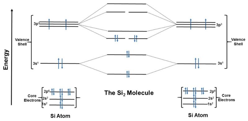
Figure 3. Relative electronic energy levels and the available molecular sub-shells in the Si2 molecule.
Two molecular sub-shells are produced for every sub-shell in the individual silicon atom and the molecular sub-shell energy levels are arrayed above and below the energy of the corresponding atomic sub-shell, as depicted in Figure 3. Not all of the available molecular sub-shells in the Si2 molecule are needed to accommodate the valence electrons of the two silicon atoms. This is the case for all molecules; indeed, if all of the available molecular sub-shells were filled with electrons, no bonding could occur between the two Si atoms (this arises from the fact that molecular sub-shells are produced as bonding and anti-bonding pairs Ða subject that we don't need to get into in this discussion).
So, when two identical atoms combine, the available energy levels for the electrons from those atoms are doubled (the situation is somewhat more complex when two dissimilar atoms combine). Similarly, if three identical atoms combine, then there are three sub-shells generated for each sub-shell in the original atom; with four atoms, there are four sub-shells for each sub-shell in the original atom, etc. For descriptive purposes, let's use the example of a chain of n bonded hydrogen atoms each with a single available energy sub-shell to contribute to the molecule (in this case one electron in the 1s sub-shell). As atoms are progressively added to our hypothetical linear poly-hydrogen molecule, additional energy sub-shells are created between the upper and lower energy limits of the 1s shell. With each additional atom, the energy increment between sub-shells becomes smaller and the energy gap between the shells becomes slightly smaller. By the time enough atoms are added to the assemblage for it to be considered an extended solid, the number of atoms can be considered as effectively infinite. In terms of the sub-shells available for electrons within the solid, the ever-decreasing energy increment between sub-shells produces a band of available energy levels within which an electron can freely move rather than the discrete levels characteristic of isolated atoms or molecules. The continuous band of energy levels created in our hypothetical poly-hydrogen molecule corresponds to the 1s sub-shell in the isolated hydrogen atom. This band contains the accumulated electrons contributed by all of the hydrogen atoms in the molecule, creating a half-filled 1s energy band, as shown in Figure 4.
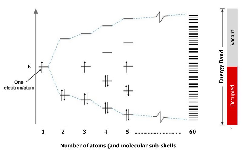
Figure 4. The arrangement of molecular energy sub-shells for a linear chain of n hydrogen atoms, each of which contains a singly occupied s orbital.
By analogy, similar molecular arrangements of heavier atoms such as silicon can produce more than one energy band through a combination of the available orbitals in the valence shell (whereas hydrogen only has a single sub-shell in the valence band, silicon has nine, four of which, the 3s and 3p sub-shells, are relevant to our discussion). When silicon atoms combine to produce the infinite atomic array that is a silicon crystal, energy bands are formed corresponding to the atomic s and p sub-shells. An examination of Figure 3 shows that the s and two of the three p sub-shells can each be expected to form an energy band that is completely filled by the available electrons. Additionally, an empty energy band, due to the vacant third p sub-shell, is also formed at an energy level relatively close to the filled p bands. These filled and empty energy bands respectively constitute the valence band and conduction band in the electronic energy model used to describe the electrical characteristics of solids.
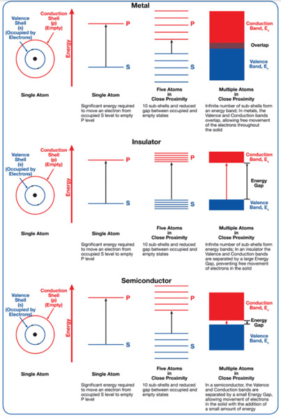
Figure 5. Electron energy band arrangement in a metal, an insulator and a semiconductor.
Figure 5 shows the relationship between filled (valence) and empty (conduction) bands in the different electrical classifications of solids. The Valence Band, denoted as Ev in Figure 5 has every sub-shell occupied by two electrons. The Conduction Band, denoted as Ec, is completely made up of vacant sub-shells. If an electron can be promoted from the Valence to the Conduction band, electrical current will flow within the solid since there are vacant sub-shells in that band that energy bands is denoted by Eg in Figure 5 and it is this gap that determines a solid material's permit electrons to flow when an electrical potential is applied. The energy gap separating these electrical properties. Figure 5 shows the band gap arrangement in a metal, a semiconductor and an insulator. The band gaps overlap in a metal so that almost no energy is required for an electron to move into the conduction band, becoming available for electrical conduction. The value of the band gap (Eg) in a metal is therefore 0, allowing free flow of electrons. In a semiconductor, the band gap is relatively small (Eg of silicon is approximately 1 electron volt, Eg in other semiconductors can be up to 2 eV) and electrons can be promoted into the conduction band by either thermal or photonic energy (hence the photoconductive behavior of semiconductors). Insulators such as glass (silicon dioxide) have large band gaps (Eg of at least 5 electron volts) and large amounts of energy are required to promote an electron into the conduction band, effectively preventing electrical conduction in these materials.
Related Topics
Semiconductor Physics
Basic Device Structures

For additional insights into semiconductor topics like this, download our free MKS Instruments Handbook: Semiconductor Devices & Process Technology
Request a Handbook Ultra-High Velocity