MOSFET Physics
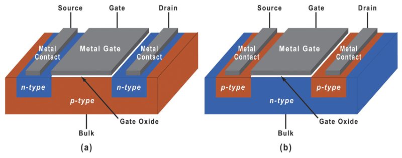
Figure 1. NMOS (a) and PMOS (b) MOSFETs.
Another very common form of transistor is the Metal Oxide Semiconductor Field Effect Transistor (MOSFET). MOSFETs are planar surface devices that are the most commonly used variant of Field Effect Transistors (FETs); the reader may also encounter Junction Gate Field Effect Transistors (JFETs) and Insulated Gate Field Effect Transistors (IGFETs). MOSFETs are actually a subset of IGFETs. FETs can replace BJTs in most electronic circuits and have advantages for use in microelectronics since they consume and dissipate less power and they can be made much smaller than equivalent BJTs. Indeed, MOSFET devices constitute the ubiquitous “bit” switch that is set to 0 (“Off” state) or 1 (“On” state) in microelectronic logic devices (i.e., computers). FETs differ from BJTs in the way that current flow through the device is controlled; the primary current flow through an FET is controlled by a small voltage applied to one of the terminals rather than by a control current flow through any part of the device. Since MOSFETs are the most widely used FET, we will use these devices to describe the components and operation of this class of transistor. Figure 1 shows the elements of a typical MOSFET where the transistor is built into the surface of a silicon bulk substrate. MOSFETs can be built as either NMOS or PMOS transistors, depending on the polarities of the bulk, source and drain regions as shown in Figure 1. The majority of carriers in NMOS devices are electrons while those in PMOS devices are holes. An NMOS device is built on a p-doped silicon substrate that has had regions of n-type material which are created using ion implantation, as shown in Figure 1(a).These n-type regions are called the source and the drain. This situation is reversed in a PMOS device, as shown in Figure 1(b). The bulk material between the source and drain in a MOSFET is called the channel. A very thin insulating oxide layer covers the channel region; it is commonly referred to as a gate oxide. Finally, a conducting gate material, either a metal or highly doped polysilicon, is deposited on top of the gate oxide, creating the three-terminal device structure shown in Figure 1.
The operational characteristics of an nMOSFET transistor are shown in Figure 2; basic operating principles of a MOSFET device can be explained within the context of an NMOS device as shown in Figure 3. Figure 3(a) shows the device in the “Off” state with the gate, source and drain voltages at zero and the bulk substrate connected to ground. Two P-N junctions exist between the n-type source/drain regions and the bulk p-type substrate. In operation, the potential between the drain and source (VDS), and that between the gate and source (VGS), are always positive. When a small voltage, (VGS) is applied to the gate, the charge carrying holes in the p-type substrate are repelled away from the substrate surface. When VGS reaches a threshold value (VTH, the minimum gate to source voltage needed to turn the device on; this is less than the 0.7 V required in BJTs, typically 0.2-0.25 V in modern logic processors), the region under the gate becomes completely depleted of charge, producing a region in the substrate called the “depletion zone”. Further increases in VGS attract electrons from the electron-rich source (VGS) and drain (VGD) regions into the region under the gate, producing an n+ region known as the “inversion layer”, shown in Figure 3(b). This inversion layer is a conducting channel that connects the two n-type regions at the source and drain; it will allow electrons to flow from the source to the drain when there is a positive voltage, VDS, between the source and drain. To assure that the induced inversion channel extends all the way from source to drain, the MOSFET gate structure slightly overlaps the edges of source and drain (the latter is achieved by a method known as a self-aligned process.
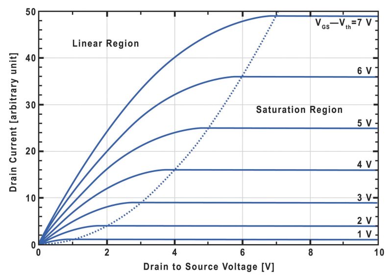
Figure 2. nMOSFET I-V characteristics.
When a drain-source bias, VDS, is applied to a NMOS device in the above threshold conducting state, electrons move in the channel inversion layer from source to drain. At relatively small values of VDS, the I/V characteristics of the device are linear with ID (drain current) increasing with increasing VD (drain voltage), as shown in Figure 3(b). Any change in the gate-source voltage VGS will alter the electron density in the inversion layer, and, in this way, changes to VGS can also control the device current. For this reason, characteristic I-V curves for NMOS devices typically depict a family of curves at different VGS, as shown in Figure 2. When the drain voltage is increased to a value known as the saturation voltage, VSAT, the charge and current flow characteristics in an NMOS device evolve, as depicted in Figure 3(c). The inversion layer under the gate becomes wedge shaped, wider (or deeper) near the source and essentially disappears (zero thickness) at the drain. This phenomenon is known as “pinch-off” and the point where the inversion layer thickness is reduced to zero is called the “pinch-off point.” Pinch-off occurs because, at VSAT, the effective potential between the gate and substrate at the source end of the channel (Veff = VGS) is greater than the potential between the gate and the substrate at the drain end of the channel, which is just the potential needed to form the inversion layer called the threshold voltage (Veff = VGS-VSAT = VTH). Any higher voltage on the drain will cause the gate to substrate voltage to be reduced below the threshold voltage and the inversion layer will not be formed, creating the pinch-off point where there are no longer any mobile electron carriers in the channel. When the voltage applied to the drain is increased beyond VSAT, the pinch-off point moves further towards the source, reducing the effective channel length, Leff, as shown in Figure 13(d). Under these conditions, the area between the pinch-off point and the drain is fully depleted with no inversion layer. Since this region has no positive free carriers, there is no possibility for electron-hole recombination if an electron enters the region from the electron-rich source and, if there is an electric field across the depletion zone, the electron can freely transit to the drain. As can be seen from Figure 2, the current through the device becomes controlled solely by the gate voltage under drain saturation conditions.
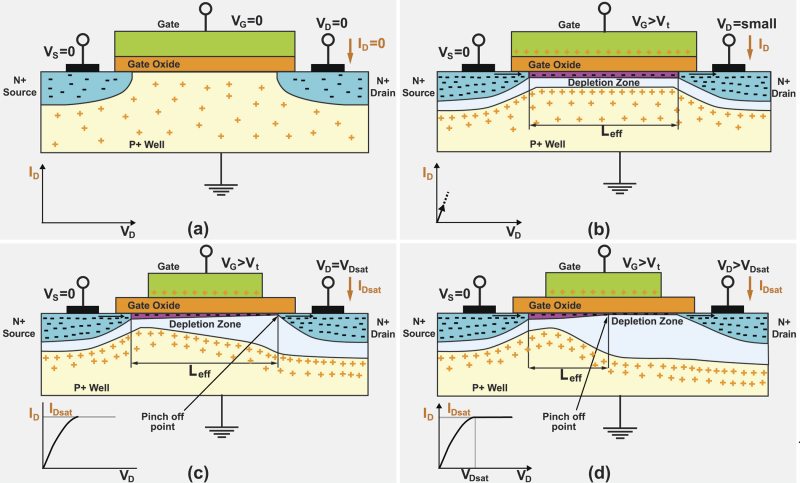
Figure 3. Operating characteristics of an NMOS field effect transistor.
Related Topics
Semiconductor Physics
Basic Device Structures

For additional insights into semiconductor topics like this, download our free MKS Instruments Handbook: Semiconductor Devices & Process Technology
Request a Handbook Ultra-High Velocity