Electrical Conduction in Semiconductors
Pure semiconductor crystals are not particularly good electrical conductors, although their conductivities are much greater than those of insulators (Table 1). The electrical property that makes semiconducting materials, and especially silicon, so valuable in electronics and other device applications arises from the fact that their electrical conductivity can be continuously varied through the controlled incorporation of dopant atoms into the crystal lattice. This property allows doped and undoped silicon to be used for the control of electrical current in a multitude of electronic devices, including diodes, capacitors and transistors. Transistors, especially, are extremely important in modern technology. They can be likened to a valve that controls the flow of electricity: a Metal-Oxide-Semiconductor Field Effect Transistor (MOSFET) device, Figure 1(a), behaves as an electrical on/off switch, while a Bipolar Junction Transistor (BJT), Figure 1(b) behaves primarily as an amplifier (controlling signals) in its linear range. Such transistors can only be fabricated using semiconductor materials.
| Material | Resistivity (Ω-cm) | Conductivity (Ω-1-m-1) |
|---|---|---|
| Insulators | ||
| Hard Rubber | 1-100 x 1013 | 1 × 10-15 to 1 × 10-13 |
| Glass | 1-10000 x 109 | 1 × 10-13 to 1 × 10⁻⁹ |
| Quartz (fused) | 7.5 x 10¹⁷ | 1.33 × 10⁻¹⁸ |
| Semiconductors | ||
| Carbon (Graphite) | 3-60 x 10-5 | 1.67 × 10³ to 3.33 × 10⁴ |
| Germanium | 1-500 x 10-3 | 2.0 to 1.00 × 10³ |
| Silicon | 0.10- 60 | 1.67 × 10⁻² to 10 |
| Metals | ||
| Silver | 1.63 x 10⁻⁸ | 6.17 × 10⁷ |
| Copper (annealed) | 1.72 x 10⁻⁸ | 5.95 × 10⁷ |
| Aluminum | 2.65 x 10⁻⁸ | 3.77 × 10⁷ |
Table 1. Relative electrical resistivities and conductivities of some metals.
Today silicon is the primary semiconducting material employed for large scale electronic device manufacturing and we will use it to illustrate the electrical properties of semiconductors. Keep in mind that the properties described for silicon can equally describe other semiconducting elements in Table 1, as well as the various compound semiconductors (GaAs, InP, etc.) that are used in more limited applications (albeit with some variation in the finer details).
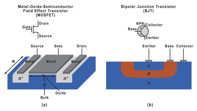
Figure 1. (a) Metal-Oxide-Semiconductor Field Effect Transistor (MOSFET) symbol and structure; (b) Bipolar Junction Transistor (BJT) symbol and structure.
Pure silicon and other elemental semiconductors are commonly referred to as intrinsic semiconductors. The term intrinsic means that electrical conductivity is an inherent property of the semiconducting material and independent of the presence of additives. In addition to intrinsic semiconductors, semiconductor device fabrication also makes use of extrinsic semiconductors (see Figure 2) that depend on the presence of dopant impurities to increase the electrical conductivity of the material. Table 1 shows the room-temperature resistivities and conductivities for a number of metals, intrinsic semiconductors and insulators. Elemental silicon has a resistivity of 0.10-60 Ω-cm—significantly higher than metallic resistivities; however, it is many orders of magnitude smaller than the resistivity of a typical insulator.
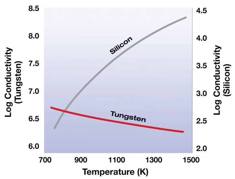
Figure 2. The electrical conductivity characteristics of a semiconductor (silicon) vs. those of a metal (tungsten).
A further difference between the electrical characteristics of semiconductors and those of metals lies in the way their conductivities vary with temperature. At absolute zero (0 K), the electrical conductivity of a semiconductor has a value of zero (i.e., the conductivity is at its minimum) whereas a metal exhibits its maximum electrical conductivity at absolute zero; furthermore, conductivity increases with increasing temperature in a semiconductor, whereas it goes down with increasing temperature in a metal. Figure 2 shows a graph comparing the temperature variation of the electrical conductivity of a semiconductor (silicon) versus a metal (tungsten). The different behaviors of electrical conductivities seen in Figure 2 can be understood in terms of the different mechanisms that govern electrical conductivity in a metal versus a semiconductor.
Metals have many free electrons available to conduct electricity. In a metal, the valence band and the conduction band overlap, so electrons are free to move into many available and vacant energy levels. When an electrical potential is applied across a piece of metal, these electrons can flow freely from higher to lower potential. The conductivity is limited only by the amount of electron scattering that occurs due to collisions between the flowing electrons and fixed atoms in the metal lattice. At 0 K, the atoms in the metal lattice are at rest and electron scattering is at its lowest possible value. As the temperature of the metal increases, thermal energy causes the atoms in the lattice to vibrate. These vibrations increase the effective diameter which an atom presents to the flow of electrons, increasing each atom’s ability to scatter electrons. Thus, as the temperature rises from 0 K, the metal atoms vibrate with continuously increasing amplitudes, increasing the degree of electron scattering and producing the observed reduction in conductivity seen in Figure 2.
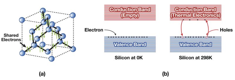
Figure 3. Silicon structure and electrical conduction.
Figure 3 can help in understanding how the mechanism of electrical current flow in a semiconductor differs from current flow in a metal. Figure 3(a) shows silicon atoms in a crystal, along with a crude schematic of how the valence electrons associated with each silicon atom are shared to produce four bonds containing eight electrons in every atom’s valence shell. As you will recall from basic chemistry, covalently bound atoms require eight electrons in their valence shell to be stable. As Figure 3(a) shows, every valence electron in a silicon atom is involved in a covalent bond and so, unlike in a metal, none are free for electrical conduction; silicon, at absolute zero, is an insulator.
Figure 3(b) shows a crude schematic of the band structure of silicon at 0 K vs. the same structure at 298 K (25°C). At 0 K, the valence band is full and the conduction band empty and there is no thermal energy available to raise a valence electron into the conduction band. As the temperature increases, the silicon absorbs thermal energy. While this energy increases the thermal vibrations of the silicon atoms (producing increased atom-electron scattering), any loss in electrical conductivity due to this phenomenon is swamped by the increase in electrical conductivity due to the thermal promotion of electrons from the valence to the conduction band. This effect is not present in metals since the conduction band overlaps the valence band. Promotion of an electron in the valence band to the conduction band creates an electron-hole pair which constitutes mobile carriers in both the conduction band (electrons) and the valence band (holes). Electrical current will now flow in the material when a potential is applied. From Figure 3(b), we can see that in an intrinsic semiconductor, there is a balance between the number of electrons in the conduction band and the number of holes in the valence band. The concept of holes is important in discussions of electronic devices because electrical current is conventionally depicted as being due to the movement of holes. Since holes represent the absence of negative charges (electrons), it is useful to think of them as positive charges. By convention, electric fields (and therefore electric potential) are depicted as a vector extending outward from areas of positive charge. Therefore, when considering current flow, electrons move in a direction opposite to the applied electric field direction (i.e., toward the positive charge), while holes move in the direction of the electric field.
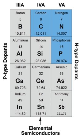
Figure 4. Elemental semiconductors and the most common n- and p-type dopants used to create extrinsic semiconductors.
When compared with metals, semiconductor electrical conductivities are not very high, as can be seen from the values in Table 1. However, semiconductor conductivities can be significantly increased (and, in fact, fine-tuned to target values) by adding impurity atoms known as dopants. “Doped” semiconductor materials are commonly referred to as extrinsic semiconductors. Figure 4 shows the area of the Periodic Table that contains the elemental semiconductors and the dopant elements that can be used to create an extrinsic semiconductor. The dopants are those elements on either side of Column IVA in the Periodic Table. A dopant atom is similar in size to the intrinsic semiconductor atom in the same row but has either one fewer or one greater electron in its valence shell. The dopant atoms can easily replace the semiconductor atom in its crystal lattice. Figure 5 shows the insertion of either a Group VA (n-type dopant, phosphorus) or a Group IIIA (p-type dopant, boron) atom into the silicon crystal lattice as well as the effect that the substitution of the silicon atom by a dopant atom has on the band structure of the silicon.
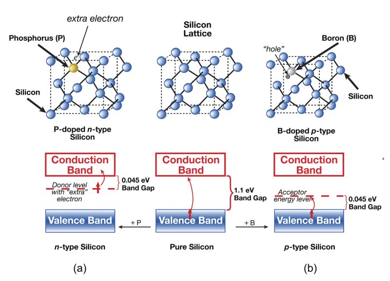
Figure 5. The effect of impurities on the band gap in extrinsic silicon.
When phosphorus, an n-type (donor) dopant is substituted for silicon, the extra electron in phosphorus’s valence shell is at a higher energy level (the donor level in Figure 5(a)) than the electrons in the filled silicon valence band. This dopant electron can easily jump the small energy gap (0.045 eV for P, much less than the 1.1 eV band gap for pure silicon at room temperature; typical donor band gaps range from .039 to .054 eV) to the empty conduction band and become a free carrier. The concentration of free carriers (and therefore the electrical conductivity) in an n-type extrinsic semiconductor is roughly proportional to the dopant concentration in the material. Since the free electron generated from dopant atoms in an n-type semiconductor does not produce a corresponding hole in the filled valence band, the dominant charge carriers in an n-type semiconductor are electrons. In a similar manner, boron can be easily substituted for silicon in the bulk crystal lattice, as shown in Figure 5(b). Since boron has one less electron than silicon, this creates a hole (an acceptor level) at an energy just greater than the top of the filled silicon valence band. Under the influence of an electric field, it takes little energy (0.045 eV for B; typical acceptor band gaps range from 0.045 to 0.160 eV) for an electron in the valence band to be promoted to this acceptor level, leaving behind a hole in the valence band. Other bound electrons in the valence band can then jump into this hole and the subsequent hole movement carries the electrical current. Thus, for p-type extrinsic semiconductors, holes are the majority charge carriers for current flow. Figure 6 shows the relationship between dopant concentration and resistivity (the inverse of conductivity) for n-and p-type dopants in crystalline silicon.
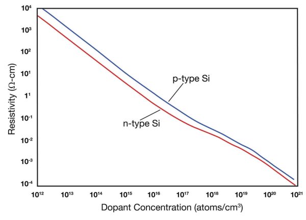
Figure 6. The dependency of the electrical resistivity at 298K on the doping concentration.
Related Topics
Semiconductor Physics
Basic Device Structures
For additional insights into semiconductor topics like this, download our free MKS Instruments Handbook: Semiconductor Devices & Process Technology
Request a Handbook Ultra-High Velocity