Flash Transistor Physics
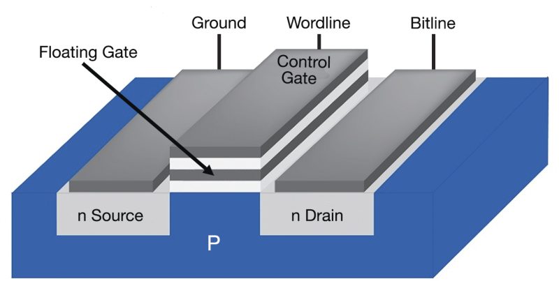
Figure 1. Flash transistor structure.
Flash transistors are used in memory devices. Their design is similar to that of MOSFETs with the main design difference being that they employ two gates rather than one in a planar MOSFET design (Figure 1). When a potential is applied to the control gate of the flash transistor, current flows between the source and drain. It differs from a conventional MOS device in that some electrons tunnel through the gate oxide to produce a permanent charge on the floating gate. The presence of this charge constitutes a logic “1” in the memory device. The charge on the floating gate can be removed by placing a negative potential on the control gate. When the floating gate has no charge, it constitutes a logic “0” in the memory device. Flash memory transistors are thus a fundamental component of most non-volatile memory devices, which are devices that maintain their charge when power is turned off.
Related Topics
Semiconductor Physics
Basic Device Structures

For additional insights into semiconductor topics like this, download our free MKS Instruments Handbook: Semiconductor Devices & Process Technology
Request a Handbook Ultra-High Velocity