Technical Notes
Filter by:
Product Category
20
9
4
3
2
2
2
1
1
1
1
Technical Notes
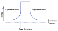
Polycrystalline Silicon Thin Films
Polysilicon thin films are produced using a process known as chemical vapor deposition or CVD. Heavily doped polysilicon and poly-silicide films have been used as gate electrodes and …
Technical Notes
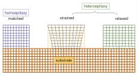
Silicon Based Epitaxial Thin Films
Epitaxy is defined as the "regularly oriented growth of one crystalline substance on another". Both homoepitaxy and heteroepitaxy processes are used in semiconductor device fabrica …
Technical Notes
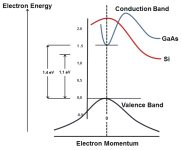
Compound Semiconductor Epitaxial Thin Films
Compound semiconductors are materials such as GaAs, AlGaAs, GaN, CdSe, InP, InSb, etc. These materials combine the elements from equidistant columns on either side of Column IVA of …
Technical Notes
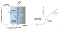
Dielectric Thin Films
Thermal SiO2 films for device components can be formed in a variety of ways; the selection of method is dependent on such factors as substrate composition/topography and the thermal …
Technical Notes
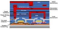
Metal Thin Films for Contacts and Interconnects
In semiconductor device fabrication, contacts are the metal components in direct contact with silicon in transistors and other devices, while interconnects are the current-carrying …
Technical Notes
Chemical Vapor Deposition Physics
Chemical vapor deposition processes can be defined as: any process in which a thin solid film is formed on a substrate by the surface-mediated reaction of adsorbed precursors from the …
Technical Notes
Semiconductor Fab Utilities Overview
Semiconductor fabrication utilities include ultrapure water, bulk high purity gases such as nitrogen and argon, exhaust gas handling and disposal, and cleanroom air systems.
Technical Notes
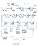
Ultrapure Water for Semiconductor Manufacturing
This technical note provides a basic familiarity with the design elements and functionalities for UPW systems. We will discuss the main UPW parameters, the treatment sequence for UPW …
Technical Notes
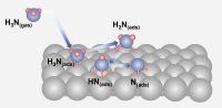
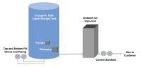
Semiconductor Gas Storage and Delivery
A variety of gases are employed for different purposes within a semiconductor device fabrication plant. These gases range from the pyrophoric and/or toxic specialty gases required for …

Technical Notes
Semiconductor Exhaust Gas Treatment
The process exhaust downstream from the cleaning, deposition and metal etch processes often experiences problems due to fouling often caused by the condensation and build-up of process …
Technical Notes
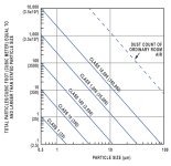
Cleanroom Ultra-clean Air Delivery
Semiconductor fab environments require ultra-clean conditions to ensure low numbers of product defects due to particulate contamination. A critical aspect in creating an ultra-clean …
Technical Notes
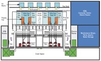
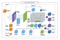
Semiconductor Process Automation
Modern 12-inch fabs have fully automated wafer processing, metrology, inspection, material handling, and device packaging with little or no human intervention between the introduction …
Technical Notes
Electrical Characteristics of Solids
When it comes to electrical characteristics, solid matter falls into one of three categories: it is either a conductor, an insulator, or a semiconductor, depending on whether or how …
Technical Notes
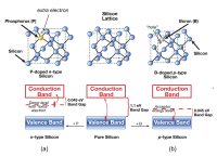
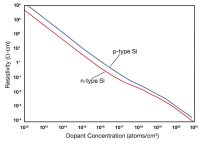
Electrical Conduction in Semiconductors
The electrical property that makes semiconducting materials so valuable in electronics applications arises from the fact that their electrical conductivity can be continuously vari …
Technical Notes
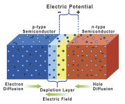
P-N Junction Physics
When p-type semiconductor and n-type semiconductor materials are placed in physical contact, the area around the contact (known as the junction) behaves differently than either of the …
Technical Notes
Diode Physics
The characteristic response of a solid state diode to an external electrical potential or to an energy source such as light forms the basis for devices such as bipolar junction transistors, …
Technical Notes
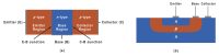
Bipolar Junction Transistor Physics
BJT operation involves both electrons and holes. It can be configured as either a PNP transistor or an NPN transistor which can be constructed as either a three-layer sandwich or as …
Technical Notes
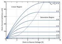
MOSFET Physics
MOSFETs are planar surface devices that are the most commonly used variant of Field Effect Transistors (FETs);including Junction Gate Field Effect Transistors (JFETs) and Insulated …
Technical Notes
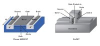
FinFET Physics
It can be seen that all of the familiar components of a MOS device are present in the FinFET (drain, source, gate, gate dielectric) and that the device more effectively separates the …
Technical Notes
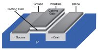
Flash Transistor Physics
Flash transistors are used in memory devices. Their design is similar to that of MOSFETs with the main design difference being that they employ two gates rather than one.
 Ultra-High Velocity