Silicon Based Epitaxial Thin Films
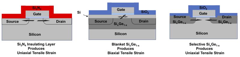
Figure 1. Biaxial and uniaxial strain techniques.
Epitaxy is defined as the "regularly oriented growth of one crystalline substance on another". Both homoepitaxy (growth of an epitaxial layer of the same material as the substrate) and heteroepitaxy (growth of an epitaxial layer composed of material that is different than the substrate) processes are used in semiconductor device fabrication. Heteroepitaxial films can be formed with either strained or relaxed lattice structures, depending on interfacial conditions and lattice parameters (Figure 1). The strain in the film can be either biaxial or uniaxial, depending on how the different materials are arranged in a device (Figure 2). Epitaxial films can be formed using a number of different methodologies, including evaporation, sputtering, molecular beam epitaxy, liquid phase epitaxy, and chemical vapor epitaxy.
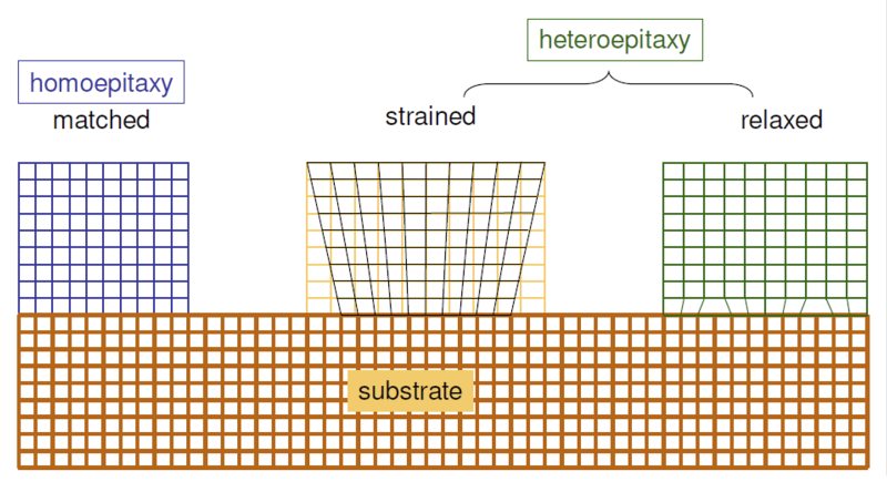
Figure 2. Epitaxial film growth modes.
Epitaxial materials are inherently freer of oxygen and carbon impurities than are bulk crystalline silicon wafers. They provide two unique advantages for device fabrication that cannot be achieved by other means:
- They offer a direct means for creating controlled and abrupt changes in dopant profiles.
- They allow the creation of strained crystalline layers that give the device designer some ability to control electron mobility by a technique known as band gap engineering
Leveraging these advantages has led to the use of silicon epitaxial layers for a variety of technological requirements in semiconductor devices.
Controlled dopant profiles and abrupt dopant profile changes offer unique advantages for device design. In bipolar devices the use of epitaxial layers to control dopant profiles enables higher switching speeds, improves high voltage operation and linearity, lowers base resistance and simplifies isolation schemes. In MOS devices, the use of epitaxial layers can lower diffused-line capacitance and improve diffused-line charge retention, improve resistance to alpha particle and static charge damage and improve dynamic Random Access Memory (RAM) performance. In addition, the use of epitaxial silicon layers in CMOS devices can improve latch-up protection. Hammond notes that Vapor Phase Epitaxy (VPE) silicon makes possible many different doping profiles that are used in modern device fabrication. These include:
- n-type silicon over p-type silicon
- p-type silicon over n-type silicon
- Lightly doped over heavily doped layers - either type
- Lightly doped over heavily doped buried layer patterns
- Conducting silicon on insulator
- Silicon layers with controlled profiles
CMOS designs that employ a lightly doped layer of epitaxial silicon over a heavily doped substrate achieve higher breakdown voltages while simultaneously keeping collector resistance low. CMOS transistor performance has also been significantly improved through the exploitation of strain-induced band-structure modification that directly impacts carrier mobility in targeted device layers. This band engineering approach leverages the enhanced electron mobility that is observed in epitaxial Si layers that are under biaxial tensile strain as well as the enhanced hole mobility that is produced in epitaxial Si1-xGex layers under biaxial compressive strain. A more intuitive way to view the influence of lattice stress on electrical conduction is to consider the impact of stress on electrons and holes. Electrons travel through the space that divides the atoms in the crystal lattice in pseudo ballistic trajectories until they encounter an electric field. Therefore, as they move through a crystal lattice, electrons are slowed by interactions with the positive electric fields surrounding each silicon atom in the lattice. When the lattice is subjected to tensile stress, the distance between atoms in the lattice is increased and electrons have longer ballistic trajectories between interactions with lattice atoms and, hence, higher mobility. Hole mobility has the opposite relationship with stress in the crystal lattice. Hole movement in the lattice is caused by an electron moving from the outer shell of a silicon atom to the outer shell of a neighboring silicon atom that has a positive charge (the hole). Basically, the hole is filled in creating a hole in the atom that donated the electron. Compressive stress reduces the distance between neighboring silicon atoms making this transfer of electron to hole easier and, in that way, increasing hole mobility. Strained epitaxial layers that are created through the use of juxtaposed Si and Si1-xGex epitaxial layers are used in the source and drain regions in advanced CMOS transistors. Channel layers in these devices also use epitaxial strained layers.
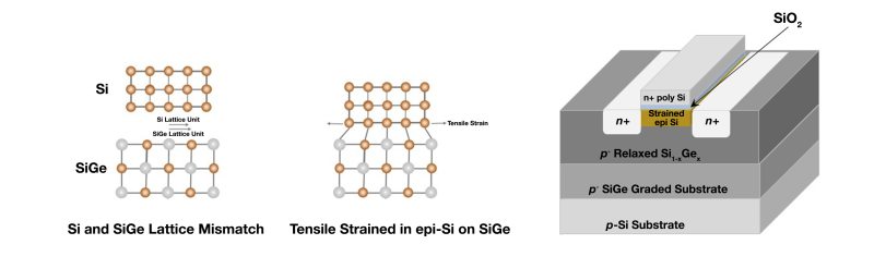
Figure 3. The origin of tensile strain in epitaxial Si/SiGe and its use in devices.
Intel was the first to use strained layer technology in high volume manufacturing of their 90 nm CMOS technology (see Figure 1). Figure 3 shows how epitaxial and other layers can be used to achieve uniaxial and biaxial strain characteristics in Intel's 90 nm CMOS transistor structure. Strained silicon epitaxial layers may also find use as enabling technology in advanced photonics applications. Table 1 provides some specifications for silicon epitaxial layers in selected device applications (from Hammond).
CVD epitaxy, also known as VPE, is the technology of choice for both homoepitaxial and heteroepitaxial processes for semiconductor device fabrication. Figure 4 shows a schematic representation of a typical VPE deposition process (for an As-doped n-epitaxial Si layer) on a wafer surface. Typically, silicon epitaxial processes are carried out at atmospheric pressure using a high flow of hydrogen carrier gas. Si1-xGex epitaxial processes differ from silicon epitaxy in that they are much more sensitive to ambient contaminants such as oxygen. Special care must be taken in these processes to employ point-of-use ultra-purification of the feed gases and/or to process under ultra-high vacuum (UHV) conditions. In addition, Si1-xGex processes are performed at significantly lower temperatures than silicon epitaxy. Recently, silicon carbide epitaxial layers have become of interest for device makers. These are higher temperature processes, running 300°C - 400°C hotter than silicon epitaxy processes.
| Device Type | Thickness (microns) | Resistivity (ohm-cm) |
|---|---|---|
| Bipolar Discrete Devices | ||
| High Frequency | 0.5-3.0 | 0.15-1.5 |
| Power | 5-100+ | 5-100+ |
| Bipolar Integrated Circuits | ||
| Digital Memory | 0.5-5 | 0.3-1.5 |
| Microprocessor | 0.5-5 | 0.3-1.5 |
| Linear | 3-15 | 2-20 |
| MOS-on-epitaxy ICs | ||
| P/P+ | 4-20 | 10-40 |
| N/N+ | 0.5-7.0 | 1-10 |
| Bipolar/MOS | 0.5-3.0 | 0.5-3.0 |
Table 1. Silicon Epitaxial layers, applications and specifications.
The chemical reactions used for the production of undoped and doped epitaxial silicon and Si1-xGex include:
- SiCl4 + 2H2 → Si + 4HCl (~1200°C)
- SiHCl3 + H2 → Si + 3HCl (~1150°C)
- SiH2Cl2 → Si + 2HCl (~1100°C)
- SiH4 → Si + 2H2 (~1050°C)
- GeH4 → Ge + 2H2
- B2H6 → 2B + 3H2
- PH3 → P + 3/2H2
- AsH3 → As + 3/2H2
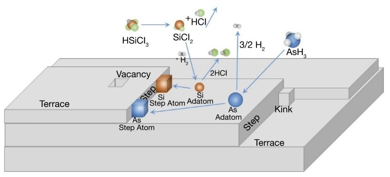
Figure 4. Schematic representations of the mechanism of epitaxial silicon layer formation.
Conventional VPE homoepitaxial processes are roughly divided into three categories: high temperature epi (1150°C - 1200°C); low temperature epi (1050°C - 1100°C); and selective epi. The heteroepitaxy processes most often encountered in device fabrication are Si1-xGex on Si, and III-V epitaxy. Reactors may operate at atmospheric pressure or under reduced pressures down to UHV. In addition, reactors may be batch-type systems (horizontal, vertical pancake and barrel reactors) that are almost exclusively used for high temperature epitaxial processes; rapid thermal processing reactors that can be employed for both high temperature (HT) and low temperature (LT) epitaxial processes; and UHV-CVD systems (developed by IBM, especially for Si1-xGex). In addition to the industry standard CVD system, physical vapor deposition is employed in molecular beam epitaxy (MBE) systems. It requires an ultrahigh vacuum environment (~10-10 Torr) and tightly controlled beams of evaporated atoms which impinge on the substrate to form the epitaxial layer. Semiconductor and dopant sources are arrayed around the substrate and shutters control the exposure of the substrate to each elemental species. Sources can be solids or gases. MBE methods are the most versatile and precise methods available for the formation of epitaxial layers. However, the exacting process requirements and the difficulty of achieving significant substrate throughput in the process have meant that this method has been largely confined to research applications and a few very advanced optoelectronic applications.
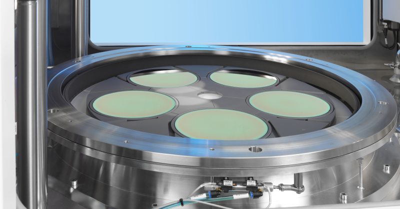
Figure 5. AIXTRON's G5+ Epitaxial Reactor.
Most modern epi processes are performed in deposition tools similar to the one shown in Figure 5. Such process tools incorporate both clean and deposit steps and allow the user to deposit sequential homo- and/or heteroepitaxial layers with customized surface preparation and minimal risk of interfacial contamination. The condition of the surface of a substrate strongly influences the perfection and hence the electrical properties of an epitaxial film. Thus the ability to control the interfacial chemical and structural properties is a necessary attribute of epitaxial process tools. Epitaxial processes require a starting substrate free of native oxide to ensure crystallinity in the epitaxial layer and to maintain high surface mobility of the adsorbed reactant species. Substrates must be pre-cleaned to remove contaminants and any native oxide on the surface and be maintained in this cleaned state until the epitaxial process has been completed. Historically, silicon homoepitaxy employed an HCl/H2 mixture as an in situ clean of the silicon substrate surface prior to the epitaxy process. Modern homo- and heteroepitaxy processes that employ chemical/mechanical polished substrates no longer require this step, and, instead, use a high temperature H2 bake to remove any native oxide from the substrate surface.
A high co-flow of hydrogen carrier gas during the epitaxial layer deposition process helps to keep the concentration of elemental reactants on the substrate surface low enough to promote ordered crystal growth; it also helps to avoid particle-producing gas phase reactions. Silicon homoepitaxial processes that employ chlorosilane precursors and temperatures in excess of 1000°C have growth rates that range between 0.2 and 2.0 µm/min, depending on the process conditions. Process temperatures in both homo- and heteroepitaxial processes are high enough to promote surface mobility of the adsorbed silicon, germanium and dopant atoms so that they move freely on the substrate surface until they become locked into an ordered crystal lattice site, as shown in Figure 5. In addition, high temperatures in epitaxial processes promote desorption of the reaction by-products from the substrate surface (i.e., HCl, H2) which, in turn, maintains high deposition rates and surface mobility.
The mechanistics of both homo- and heteroepitaxial process can be roughly broken down into the following steps, illustrated in Figure 4:
- transport of the reactants to the deposition region
- transport of the reactants by diffusion from the main gas stream, through the boundary layer next to the substrate surface
- adsorption of the reactants on the substrate surface
- surface processes: migration, decomposition, reaction and site incorporation
- desorption of by-products from the surface
- transport of by-products through the boundary layer
- transport of by-products out of the deposition region
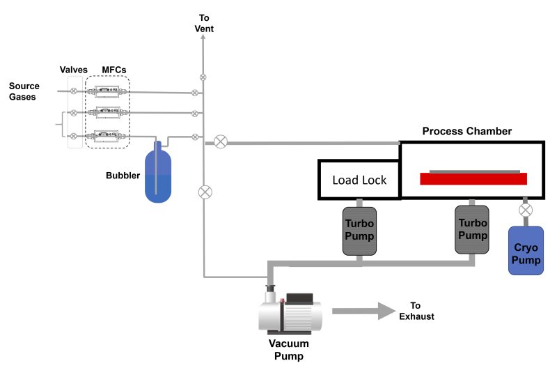
Figure 6. Schematic of a UHV-CVD Epitaxial Reactor.
The development of epitaxial processes for Si/Si1-xGex hetero- and quantum well structures requires low temperature processing to avoid diffusion and intermixing at the Si- Si1-xGex interfaces. The silicon and germanium sources used in Si1-xGex epitaxy are normally silane, SiH4, and germane, GeH4; compounds that begin to decompose at process temperatures of 500°C (some Si1-xGex processes use chlorosilanes and require somewhat higher temperatures). The assumption that extremely low vapor pressures of water and oxygen in the gas phase are required in Si CVD epitaxy processes stimulated the development of the UHV-CVD epi processes in the late 1980s. It was found that the minimum temperature, in general, for epitaxial processes was lower for UHV-CVD with films deposited at temperatures less than 500°C. However, the relatively high cost associated with the technique tends to restrict its application to those areas with no other option. Si1-xGex processes in UHV-CVD reactors can be configured to operate as batch processes and Figure 6 shows a schematic view of such a UHV-CVD system. A turbomolecular pump combined with a roots blower and a mechanical pump in series are used to achieve UHV conditions, typically with base pressures of <10-9 Torr. As with conventional epitaxial processes, hydrogen is used as a carrier gas, silane and germane are the reactive gases and B2H6 and PH3 are mixed into the gas flow for p- and n-type doping of the epitaxial layers. UHV-CVD epitaxial Si1-xGex films are grown at deposition temperatures ranging from 450°C - 520°C. At higher deposition temperatures the hydrogen passivation of the substrate desorbs and a clean wafer surface cannot be maintained. High temperature bakes such as those in conventional silicon epitaxial processes are not possible in UHV systems due to the limits of the system components. With wet chemical cleaning, including an HF dip for surface H-passivation, and rapid transfer to the deposition chamber, the Si/Si1-xGex interface typically shows oxygen and carbon contamination in the range of 1010 to 1012 atoms/cm2. The silicon surface atom density is 7 x 10¹⁴ atoms/cm2, which means that less than one atom in a thousand at the interface is a contaminant.
Related Topics
Thin Films
- Polycrystalline Silicon Thin Films
- Compund Semiconductor Epitaxial Thin Films
- Dielectric Thin Films
- Metal Thin Films
Thin Film Deposition
For additional insights into semiconductor topics like this, download our free MKS Instruments Handbook: Semiconductor Devices & Process Technology
Request a Handbook Ultra-High Velocity