Dielectric Thin Films
Silicon Dioxide
Insulating thin films of silicon dioxide SiO2 are uniquely critical materials within silicon semiconductor device technology since they are major components in all MOS devices, as well as in other metal-insulator-semiconductor (MIS) and tunneling structures. For instance: thermal grown oxides are employed as sacrificial protective layers and masks for substrate doping; thick thermal oxide films are used as isolating field oxides in devices with relatively large design rules (thermal oxide use in this application has been largely supplanted by deposited oxides and trench isolation in nanometer scale devices); and thin oxide films are used as gate oxides or gate oxide components in more advanced devices, albeit supplemented by high-k ALD deposited materials.
Thermal SiO2 films for device components can be formed in a variety of ways; the selection of method is dependent on such factors as substrate composition/topography and the thermal tolerances of other device features on the substrate. Methods for producing SiO2 films include thermal oxidation of silicon, PECVD, LPCVD, APCVD, MOCVD, and PVD. The chemistries range from simple oxygen-based reactions to the complex organometallic chemistry used in MOCVD. Of these methods, the thermal oxidation of silicon produces the highest quality insulators.
The availability of an adherent, impermeable, high dielectric strength thermal oxide is, arguably, the reason that silicon technology has dominated semiconductor device design and microelectronics manufacturing for the past 50 years. Other materials such as germanium and GaAs have superior electrical properties when compared with silicon; indeed, germanium was selected as the substrate in the first transistor design. However, neither of these materials nor any other likely candidates except silicon has a well-behaved insulating oxide that can be grown on the substrate by simple thermal oxidation in large batch processes. It is this single attribute that has allowed silicon technology to dominate the microelectronics world for so long.
| DC Resistivity (Ω-cm, 25°C) | > 1020 |
| Density (g/cm3) | 2.27 |
| Dielectric Constant | 3.8 - 3.9 |
| Dielectric Strength (V/cm) | 5 - 10 x 106 |
| Energy Gap (eV) | ~9 |
| Etch Rate (BOE, Å/min) | 1000 |
| Linear Expansion Coefficient (cm/cm ¡C) | 5.0 x 10⁻⁷ |
| Melting Point (°C) | ~1700 |
| Molecular Weight | 60.08 |
| Molecules/cm3 | 2.3 x 10²² |
| Refractive Index | 1.46 |
| Specific Heat (J/g°C) | 1.0 |
| Stress in film on Si (dyne/cm2) | 2 - 4 x 10⁹ |
| Thermal Conductivity (W/cm °C) | 0.014 |
Table 1. Selected physical constants of thermally grown silicon dioxide. Taken from "Silicon Processing for the VLSI Era", Stanley Wolf and Richard N. Tauber, Lattice Press, 1986.
Table 1 is a table taken from Wolf and Tauber. It contains selected physical properties of silicon dioxide that are relevant to its use in semiconductor device manufacture. It can be seen that thermal oxide has excellent electrical properties for use as an insulator in microelectronic devices. It exhibits very high resistivity, but, more importantly, it has a high breakdown electric field strength. The large energy gap provides good protection from tunneling, at least down to nanometer-scale thicknesses. Physically, thermally grown oxides are stable with reproducible Si/SiO2 interfaces, an important factor in device fabrication at low nanometer dimensions. Finally, the oxide can be grown in a conformal manner over varied topography on the silicon surface. This means that insulating films produced by thermal oxidation will not exhibit thin spots at sharp edges and corners in the underlying topology, obviously important for good electrical insulation in a device. Silicon dioxide thin films are an amorphous form of silica consisting of SiO4 tetrahedra linked together through all four oxygen atoms. The term amorphous means that the films do not have a well-defined crystal structure, having only short range order in their molecular components.
Silicon can be thermally oxidized using either dry oxygen or steam. Dry oxidation is typically used for films having thicknesses of less than 100 nm since growth occurs more slowly (and thus more controllably) in the dry process (typically 14 - 25 nm/hour). Wet oxidation uses steam as the oxidant and exhibits significantly higher growth rates (100 - 200 nm/hour). Wet oxidation is preferred for the formation of thicker films, up to 1000 nm. Dry oxidation, however, produces a higher quality oxide than wet oxidation since films formed using the latter process have significant concentrations of hydroxyl groups, OH-, both in the bulk film and at the Si/SiO2 interface. This degrades their electrical properties as compared to those of "dry" oxides. Note that advanced methods such as in situ steam generation (ISSG) at low pressures (< 20 Torr) resolve some of the purity issues of wet oxides and these processes have found use for ultra-thin gate oxidation and shallow trench isolation liners. Figure 1(a) provides a schematic that identifies the key physical and chemical aspects of the thermal oxidation of silicon while Figure 1(b) shows a typical equipment arrangement for the process (in this case ISSG).
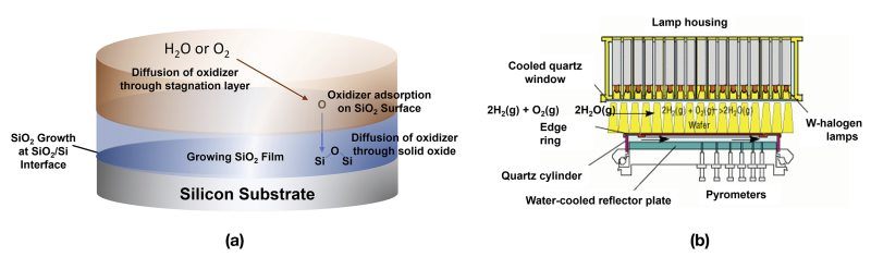
Figure 1. Thermal silicon oxidation: a) Process b) Equipment configuration (Reproduced with permission of Solid State Technology).
Since the simplest oxidation chemistry is that associated with dry oxidation and since, in general, it produces the highest quality thermal oxide, we will use this process as the basis for a discussion of how silicon is oxidized and the characteristics of the film produced by the oxidation. The growth process of silicon oxidation has been extensively studied over the past 50 years. While the chemistry can be simply expressed:
Si + O2 → SiO2
the kinetics of the process and the structure of the film and interface are far from simple. The oxidation process occurs at the Si/SiO2 interface and the rate of the oxidation is determined by a complex relationship between the concentration of oxygen in the gas and on the surface of the growing film, the rate of diffusion of oxygen through the growing oxide film, and the chemical reaction between oxygen and silicon at the interface. Since the reaction consumes silicon, the interface continually moves into the silicon substrate during the oxidation process, with Si-Si bonds being broken and new Si-O bonds formed. This complicates the kinetics, since it causes the oxygen diffusion times and concentration of oxygen at the interface to vary with time. Also, the transition from the tightly ordered crystal lattice of silicon to the more open amorphous structure of silicon dioxide produces a volume expansion of the substrate/oxide film system as the oxide film grows. In the final structure, about 46% of the silicon dioxide that is grown is found within the bounds of the original silicon while 54% of the oxide is new volume. An understanding of all of these factors is critical in the device fabrication process since they must be quantitatively known or estimated for precision in gate oxide processing at the nanometer scale.
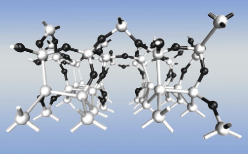
Figure 2. A model of the Si/SiO2 interface; grey balls represent silicon atoms, black balls represent oxygen atoms.
The nature of the interface between the silicon substrate and the silicon dioxide film (Figure 2) in thermally grown gate oxides is also a critical parameter since it strongly influences the operational characteristics of transistors at nanometer dimensions. The interface is not perfect at the atomic level, but rather a randomized transition from Si - Si to Si - O bonding. Interfacial zones that are as close to perfect at the atomic level are sought in the manufacturing process in order to achieve optimal device performance since the greater the perfection of the interface, the more predictable and repeatable are the electrical properties in devices. Many studies have been performed over the past few decades in an effort to understand and control the character of the interface and to limit the impact of imperfections on device performance. Much work has gone into finding process and equipment approaches to improve this interface.
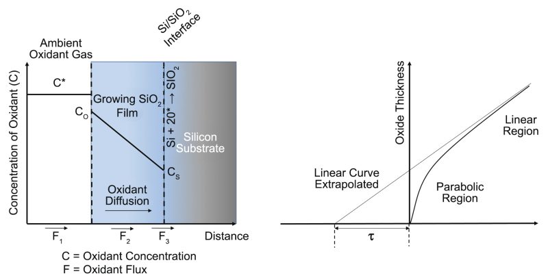
Figure 3. One-dimensional Deal-Grove model for the oxidation of silicon.
The growth process of thermal SiO2 films has been extensively modeled and experimentally evaluated. Almost all models of the process begin with the model developed by Bruce Deal and Andy Grove in 1965. They proposed that the oxidation rate was determined by the combination of two processes. The first involved the actual chemical reaction of oxygen with silicon at the oxide/substrate interface, while the second was the diffusion of oxygen through the previously formed oxide film. The combination of these processes resulted in the formulation of the classical "linear-parabolic" rate law of Deal and Grove (Figure 3):
dx/dt = F/N1 = (kC*/N1) / (1 + k/ℎ + kℎ/Deff)
where x is the oxide thickness, F the total flux of oxidant molecules through the oxide, k the first-order rate constant for the oxidation reaction, C* the concentration of oxidant at the oxide surface, N1 the number of oxidant molecules incorporated into a unit volume of the oxide layer, ℎ the gas phase transport coefficient of oxygen, and Deff the effective diffusion coefficient of oxygen in silicon dioxide. When the differential equation is solved, the above equation can be rewritten as:
x2 + Ax = B(t + τ)
where
A =2Deff(1/k + 1/ℎ)
B = 2DeffC*/N1
and
τ = (x02 + Ax0)/B
The Deal-Grove model requires the parameter τ (a shift in the time coordinate) in order to account for the presence of an initial oxide layer on the silicon surface. This approach was found to provide an excellent fit to experimental data for oxidation processes utilizing H2O/O2 mixtures and for dry oxidation processes at thicknesses in excess of approximately 40 nm. Deal-Grove estimates fail, however, in predicting oxidation rates in dry oxygen within the thin regime (<20 nm) and in accounting for the observed pressure dependence of both thin and thick oxidations. Within the thin regime, observed oxidation rates in dry processes are significantly greater than Deal-Grove predictions and the reaction exhibits a power law dependence on the oxygen pressure with rate proportional to Pm where m = 0.6-0.8. It is beyond the scope of this overview to detail the refinements to the Deal-Grove model that have occurred over the past few decades. In 1995, one author wrote in a publication on thermal oxidation kinetics An examination of the literature and available experimental evidence does not permit a definitive choice of model for the oxidation of silicon. A review of the literature since that time suggests that, while our understanding has improved, the thermal oxidation kinetics remains a valid field of study.
Deposited Silicon Dioxide Thin Films
Silicon dioxide thin films can be deposited under a variety of conditions and using a variety of chemistries. Over the past half century, silicon dioxide films have been deposited using reaction conditions that varied from atmospheric pressure through sub-atmospheric pressures (SACVD) to low, vacuum pressures (LPCVD and PECVD). The reactions that produced the oxide film have been both thermal and plasma-enhanced. The chemistries employed in the deposition processes have varied. In this section, we will describe a few of these routes to deposited silicon dioxide films and the properties of the films produced.
Silane-Based Oxides (Low Temperature Oxide, LTO)
For much of the past 50 years, the most widely used deposited silicon dioxide film processes have used the reaction of silane with oxygen or a milder oxidant such as nitrous oxide, N2O. The primary advantage of hydride-based deposited silicon dioxide films is the low deposition temperature, compatible with aluminum metallization. The chemistry for the deposition processes are relatively simple:
SiH4 + 2O2 → SiO2 + 2H2O
SiH4 + 2N2O → SiO2 + 2N2 + 2H2
The first of these processes is usually thermally driven while the second is normally plasma enhanced; both were originally batch processes, depositing oxide films on up to a hundred wafers at a time, however they have been adapted to single wafer processing environments. Process temperatures are in the 200 - 450°C range with PECVD reactions normally performed at the lowest temperatures. These processes have noteworthy safety risks since the precursor, silane, is a high pressure, pyrophoric gas. This means that, should the gas leak from its high pressure cylinder, it will spontaneously burst into flame or, under certain conditions, explode. There have been a number of lethal accidents in the semiconductor industry associated with silane and safety precautions are critical in its handling.
While the chemistry of hydride-based silicon dioxide deposition can be summarized by relatively simple reactions, the detailed chemistry that occurs in these systems is actually quite complex. Under the pressure and temperature conditions employed in all of the hydride-based oxide deposition processes (SACVD, LPCVD and PECVD) unstable reactive intermediate species formed in the gas phase make a significant contribution to the overall deposition process. Reactive intermediates are formed by reactions such as:
SiH4 + O2 → SiH2(OH)2
SiH4 + H2O → SiH3OH + H2
SiH4 + N2O → SiH3OH + N2
The formation of silanols, SiHx(OH)4-x, is chemically favored (ΔHf(SiH2(OH)2) ~ -100 kcal/mol) in this system. They are highly reactive chemical species that further react to produce SiO2 once adsorbed on the substrate surface. The presence of reactive silanol intermediates in these deposition processes has major consequences for both the equipment requirements and the materials properties of the oxide films produced. The equipment used in the deposition processes, especially for the LPCVD process, must be configured with precise surface area/volume relationships between the surface of the substrate, the spacing of substrates in batch processes, and the surfaces surrounding substrate edges. If these relationships are not maintained, the uniformity of the thin oxide film over the substrate surface can be seriously degraded. Additionally, silanols in the gas phase readily react with other silanols and with silane to produce gas phase particulates that are extremely damaging to device yields. As with film uniformity issues, control of gas phase nucleation in the reactions is strongly dependent on reactor geometry and surface-to-volume rations in the reaction chamber.
| Deposition | Thermal | LPCVD/APCVD LTO (Densified) | LPCVD/APCVD TEOS (as deposited) | HTO | PECVD |
|---|---|---|---|---|---|
| Source | O2 | SiH4 + O2 | TEOS + O2 | SiCl2H2 + N2O | SiH4 + N2O |
| Temperature (¡C) | 900-1000 | 400-450 | 700 | 900 | 200-400 |
| Composition | SiO2 | SiO2(H) | SiO2 | SiO2(Cl) | SiO2(H) |
| Step Coverage | Conformal | Nonconformal | Conformal | Conformal | Nonconformal |
| Thermal Stability | Stable | Densifies | Stable | Loses Cl | Loses H |
| Dielectric Constant | 3.9 | 4.1 | 4.3 | - | 6-9 |
| Dielectric Strength (MV/cm) | 10 | 6-7 | 5-6 | - | 7 |
| Density (g/cm3) | 2.2 | 2.1 | 2.2 | 2.2 | 2.3 |
| Density (g/cm3) | 3 Compressive | 3 Tensile | 1 Compressive | 3 Compressive | 3 Compressive to 3 Tensile |
Table 2. Comparison of different silicon dioxide processes and properties.
The as-deposited materials properties of LTO (silane-based) silicon dioxide films deposited in these processes are distinctly inferior to those of thermal silicon dioxide films. Films of these materials have to be densified after deposition and, even following densification, significant quantities of Si-OH and Si-H remain in the film. The result of this contamination is a dielectric strength for deposited films that is significantly weaker than that of thermal oxides, typically 6-7 MV/cm (vs. approximately 10 MV/cm for thermal oxide). These films cannot, therefore, be used in applications requiring high electrical integrity such as gate oxides. Therefore, their material property limitations have historically restricted their use in device fabrication to the formation of insulating layers between the active layer on the substrate and the different levels of metal in the device. In nanometer-scale device structures, however, intermetal dielectric films require almost perfect conformality in the deposited films, a property that LTO films lack. The term conformality refers to the uniformity of coverage over sharp edges and deep trenches in the substrate topography. Figure 4 illustrates good vs. poor conformality characteristics. The poor conformality of hydride-based silicon dioxide processes has led to their being largely supplanted by TetraEthOxySilane (TEOS, sometimes also called TetraEthylOrthoSilicate) and TEOS/O3 processes. Table 2 provides a comparison of some of the critical properties of LTO films compared with other silicon dioxide thin film sources.
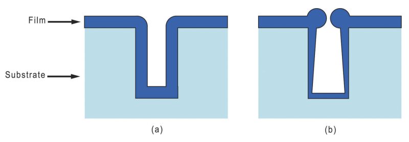
Figure 4. Deposited film conformality: a) conformal film; b) nonconformal film.
High Temperature Oxide (HTO)
High temperature silicon dioxide (HTO) films are formed by the reaction of dichlorosilane and nitrous oxide:
SiH2Cl2 + 2N2O → SiO2 + 2N2 + 2HCl
HTO processes are carried out at high temperatures, typically around 900°C and under low pressure conditions, typically around 200 mTorr process pressure. The high process temperature results in an oxide that is very close to thermal oxide in many of its properties (Table 2). However, the high process temperature also limits the utility of HTO, since dopant migration and loss of metal line integrity become problems. In addition, the presence of chlorine as a contaminant in HTO can be a problem. For these reasons, HTO films do not have an extensive list of applications in device fabrication. However, the use of rapid thermal processing techniques with very short time at temperature has raised interest in the use of HTO as a replacement for Oxide-Nitride-Oxide (ONO) films as interpoly dielectrics in flash cells and gate dielectrics.
TEOS-Based Oxides
TEOS-based oxides have largely supplanted LTO as passivation and intermetal dielectric films in device manufacture. The TEOS molecule has the chemical formulation Si(OC2H5)4. Formally, TEOS is an organometallic compound and TEOS-based deposition processes can be classed as MOCVD, although this is rarely noted as such.
Early use of TEOS-oxides employed LPCVD batch processing and simple thermal decomposition of the TEOS molecule:
Si(OC2H5)4 [700°C]→ SiO2 + 4C2H4 + 2H2O
In practice, the process usually required a small amount of co-reactant oxygen for good process characteristics such as film uniformity and low particle counts. The LPCVD TEOS process produced a very stable silicon dioxide film with properties approaching those of thermal oxide (Table 2). More importantly, the films exhibited excellent conformality, able to uniformly cover relatively severe surface topographies to produce an excellent interpoly dielectric.
The process temperature requirements of LPCVD TEOS-oxide processes limited their use as intermetal dielectrics, so PECVD-based TEOS oxide processes were quickly developed to fill this need. PECVD TEOS-oxide processes exhibit high deposition rates at low deposition temperatures while simultaneously producing oxide films having excellent conformality. The low deposition temperatures (200°C-400°C) allow these processes to be used for the deposition of intermetal dielectrics. Unfortunately, the low deposition temperature can be problematic for film quality, yielding oxide films that are hygroscopic and containing significant structural and electrical defects and some process modifications and/or post-deposition processing may be required to raise the film quality to acceptable levels.
More recently, TEOS/O3 processes have been developed that produce excellent silicon dioxide films for intermetal dielectric applications. Originally, TEOS/O3 was developed as LPCVD and APCVD processes; the most successful variant on TEOS/O3 has been the subatmospheric pressure CVD (SACVD) TEOS/O3 process. SACVD TEOS/O3 processes deposit highly conformal, high quality silicon dioxide films at process pressures ranging from 100 Torr to 600 Torr and temperatures as low as 300°C, allowing their use in all interlevel insulation applications. The process chemistry can be simply written as:
Si(OC2H5)4 + O3 → SiO2 + 2C2H6 + 2C2H4O + 5/2O2
however, it is actually much more complex.
Silicon Nitride
3SiH2Cl2 + 4NH3 → Si3N4 + 6HCl + 6H2
In practice, HCl is undesirable in the process effluent since it can cause severe corrosion in the downstream components and therefore, a sufficient excess of ammonia is added to the process to ensure that the reaction chemistry is:
3SiH2Cl2 + 10NH3 → Si3N4 + 6NH4Cl + 6H2
The presence of NH4Cl in the process effluent can also be detrimental to the maintenance requirements of the deposition system (although not as bad as HCl). LPCVD silicon nitride processes require high temperatures, typically in excess of 700°C, while PECVD nitride can be deposited at temperatures below 400°C. The usual trade-off between process temperature and film quality exists for these two processes, with the LPCVD process producing a high quality, stoichiometric film and the PECVD process producing a non-stoichiometric film containing varying concentrations of silicon-hydrogen bonds.
Silicon nitride films are amorphous, hard materials that find two primary uses in device manufacture: masking layers and final passivation. Masking layers are typically deposited using LPCVD since this produces the most impervious film. Silicon nitride masking layers are especially useful for thermal oxidation processes since oxygen does not easily diffuse through the nitride. Silicon nitride has a number of desirable qualities as a passivation layer. PECVD methods allow it to be deposited at temperatures compatible with the underlying device structures. The film is nearly impervious to critical ambient contaminants such as moisture and sodium. Finally, by adjusting the PECVD process conditions the inherent stress in the film can also be adjusted to eliminate any risk of film delamination or cracking. As will be discussed later, silicon nitride finds use as a stop for chemical mechanical polishing processes. Table 3 provides a list of representative properties of LPCVD and PECVD silicon nitride thin films.
| Property | LPCVD Si3N4 | PECVD Si3N4 |
|---|---|---|
| Composition | Si3N4 | SixNyHz |
| Density (g/cm3) | 2.8 - 3.1 | 2.5 - 2.8 |
| Dielectric Constant | 6 - 7 | 6 - 9 |
| Dielectric Strength (MV/cm) | 10 | 0.6 |
| Bulk Resistivity (Ω-cm) | 1015 - 1017 | 1015 |
| Stress (dyne/cm2) | 1.8 x 10¹⁰ (tensile) | 8 x 10⁹ (compressive) |
Table 3. Representative properties of LPCVD vs. PECVD silicon nitride.
High-k and Low-k Dielectrics
The dielectric constant (k) of a material is a measure of the polarizability of that material. In a dielectric, polarization can have three origins. An external electric field can induce electronic polarization in which the electrons in neutral atoms are displaced from a symmetrical arrangement around the nucleus. It can also induce atomic or ionic polarization in which adjacent positive and negative ions are distorted from their equilibrium positions in a crystal lattice. Finally, it may cause dipolar or orientational polarization in which permanent dipoles in a material align with the external electric field. Low dielectric constant (low-k) materials exhibit weak polarization when subjected to an applied electric field; high-k materials are strongly polarized in the presence of an external electric field.
Over the past two decades, materials having dielectric constants (k-values) that are both higher and lower than those of conventional silicon dioxide and silicon nitride have become increasingly important in device manufacturing. Low-k materials are important for the reduction of Resistance-Capacitance (RC) delays in interconnects. High-k materials are important for use in storage capacitors and nonvolatile memory devices, and have become a critical component that allows continued scaling in the ultra-thin film stacks employed as gate insulators in nanometer scale devices.
Low-k materials, when used as insulators between the multilevel interconnections in a device, have the ability to improve device speed through reductions in RC delays. RC effects occur due to the unintended formation of capacitor structures when two metal interconnects are separated by an insulating layer. When this occurs, there is a delay in the transmission time of interconnect signals that is proportional to the time it takes to charge the incidental (parasitic) capacitor. This time, denoted by the symbol ., is equal to the resistance of the interconnect times the capacitance of the incidental capacitor. This capacitance is, in turn, directly proportional to the dielectric constant of the insulating material and the area of the incidental capacitor and inversely proportional to the distance between the metal lines. Thus, as the distance between metal lines in multilevel metal structures is reduced, the delay in signal transmission increases unless the dielectric constant of the material separating the metal lines can be reduced.
Historically, the insulator used to separate metal lines in a device (the inter-level dielectric, ILD) has been SiO2 which has a dielectric constant of about 3.9. By way of comparison, the lowest possible dielectric constant is 1.0 (vacuum or air). Materials for ILD applications have been specifically designed for the reduction of their dielectric constant. In general, the design principals focus on the reduction of any chemical characteristics that can result in moisture absorption and in designing the molecular chemistry to reduce polarization strength and density. This latter characteristic can be accomplished by reducing the Si-O bond density in the material and through the incorporation of fluorine (SiOF dielectric constant = 3.7) and organic species such as CH3 (SiOC(H) dielectric constant = 2.8).
| Dielectric Material | Dielectric Constant |
|---|---|
| Silicon Dioxide SiO2 | 3.9 |
| Silicon Nitride Si3N4 | 7-8 |
| Aluminum Oxide Al2O3 | 8-10 |
| Hafnium Oxide HfO2 | 25 |
| Titanium Oxide TiO2 | 30-80 |
| Zirconium Oxide ZrO2 | 25 |
| Tantalum Pentoxide Ta2O5 | 25-50 |
| Barium-strontium-titanate BST | 100-800 |
| Strontium-titanate-oxide STO | 230+ |
| Lead-zirconium-titanate PZT | 400-1500 |
Table 4. High dielectric constant materials.
Many materials with dielectric constants lying between the limits of air and SiO2 have been evaluated as ILDs over the past few decades. CVD methods have been employed to deposit carbon-doped silicon oxide and organosilicate glass, OSG. These methods have produced ILDs with dielectric constants as low as 2.5, albeit with decreasing mechanical strength in the films. Spin-on hydrocarbon and fluorocarbon polymers have been evaluated, including polyimides, polyarylethers (PAE), polynorbornene and polytetrafluoroethylene (PTFE). These materials typically exhibit dielectric constants around 2.5. However, they tend to have weak mechanical strength, poor thermal stability and poor adhesion. Mixed organic/inorganic silicon based polymers having very open lattice structures, collectively known as polysilsequioxanes (SSQ), have also been evaluated. Most recently, the very low dielectric constant of air (1.0) has been leveraged for ILD dielectric constant reduction through both direct use and the use of highly porous materials for ILDs. Air gaps have also been used in both logic interconnects and DRAM devices. The latter materials include porous silicate glass, xerogel/aerogel, porous organosilicate glass, porous SSQ, porous organics and porous SiLK (a trademarked porous organic polymer). These materials are normally applied using a spin-on sol-gel process followed by heat treatment to remove the solvent.
High-k gate dielectric materials, mainly transmission metal oxides, have proven crucial for successful device operation at device feature sizes of 65 nm and below. At these dimensions, the gate oxide in Field Effect Transistors, if fabricated from SiO2, must have a thickness of 0.7 nm. This is much less than the direct electron tunneling thickness for SiO2 films of 3.0 nm. This means that electrons can "tunnel" through such thin oxides to produce gate leakage currents of about 100 A/cm2 at 1V. Obviously, such large leakage currents effectively destroy the transistor functionality. The use of high-k materials as part of the transistor gate structure avoids this problem since the high degree of polarizability of these materials allows low electrical potentials on the gate to more strongly influence the underlying channel. Table 10 provides dielectric constant values for some high-k materials of interest to the semiconductor community.
Silicon Oxynitride, SiOxNy
Silicon oxynitride was one of the first high-k materials to be explored in the quest to avoid excessive leakage through ultra-thin gate insulators. SiOxNmks has the additional benefit of improved barrier performance for boron penetration in surface-channel P-MOSFETs that have P+ gate electrode doping. Silicon oxynitride is a compromise in that silicon nitride provides better material characteristics; however, the deposition process for silicon nitride produces a high density of traps in the film, making it unsuitable for use as a gate dielectric. SiOxNy films can exhibit dielectric constants up to around 5.0, as compared with silicon dioxide values of 3.9. Currently, SiOxNy materials are of interest as gate insulators for conventional device fabrication and as components having tunable refractive indices for photonics application.
Silicon oxynitride films can be formed on the substrate using a number of simple, accessible chemical approaches:
- Thermal nitridation of silicon followed by re-oxidation
- Annealing of SiO2 films in nitrogen-containing ambient such as nitrous oxide (N2O), nitric oxide (NO2) or ammonia (NH3)
- Growth of SiO2 on nitrogen implanted substrates
- Low temperature remote plasma nitridation of SiO2
- ALD nitride deposited on SiO2
- PECVD, CVD
Using electron cyclotron resonance (ECR) remote plasma reactors, SiOxNy can be deposited at low temperatures and with minimal damage to the gate insulator-substrate interface with the substrate. ECR PECVD approaches allow for relatively precise control of oxygen to nitrogen ratios, low S-H concentrations, good uniformity and microstructure control in the SiOxNy film. Approach (e) has received recent attention as a preferred route to SiOxNy formation.
Aluminum Oxide, Al2O3
Aluminum oxide is another material of potential interest as a gate insulator, especially for thin film transistors (TFTs) on glass and flexible substrates, owing to its high dielectric constant (~9), relatively low leakage current and good thermal/electrical stability. To be of use in modern device fabrication, and especially for applications on flexible substrates, Al2O3 films must be deposited at quite low temperatures. Conventional PVD and CVD deposition approaches for Al2O3 at low temperatures have not produced films with acceptable properties for device applications. The films exhibit high leakage and poor stability due to the grainy growth and rough, polycrystalline surfaces. ALD methods, however, have proven to produce excellent films for TFT gate insulator applications. ALD processes for Al2O3 film deposition can be performed at temperatures as low as 120°C, making them ideal for the production of TFTs on flexible substrates and as a blocking dielectric in memory devices. Al2O3 is also used in non-volatile memory applications such as 3D-NAND.
Related Topics
Thin Films
- Polycrystalline Silicon Thin Films
- Silicon Based Epitaxial Thin Films
- Compund Semiconductor Epitaxial Thin Films
- Metal Thin Films
Thin Film Deposition

For additional insights into semiconductor topics like this, download our free MKS Instruments Handbook: Semiconductor Devices & Process Technology
Request a Handbook Ultra-High Velocity