Chemical Vapor Deposition Physics
Chemical vapor deposition processes can be defined as: any process in which a thin solid film is formed on a substrate by the surface-mediated reaction of adsorbed precursors from the gas phase. The reactive nature of CVD processes distinguishes them from physical processes such as evaporation and sputtering that are employed in PVD. The term "surface-mediated" refers to the fact that the solid film is formed by a heterogeneous reaction occurring at the substrate surface. The chemical compounds that react on the surface can be either the original reagent chemicals fed to the system or short-lived intermediate species created in the high temperature gas phase. As a general rule, most CVD processes and equipment are designed so as to avoid the formation of such gas phase intermediate species, since they can self-react to produce gas phase particulates. Historically, most CVD processes were carried out using batch reactor approaches in either horizontal, hot-wall tube reactors under vacuum or in continuous reactors at atmospheric pressure. As device sizes shrank, however, the need for tighter control over the chemical processes in CVD reactions became ever more critical, leading to a greater prevalence today of single wafer/cluster tool equipment configurations in which thin films can be grown.
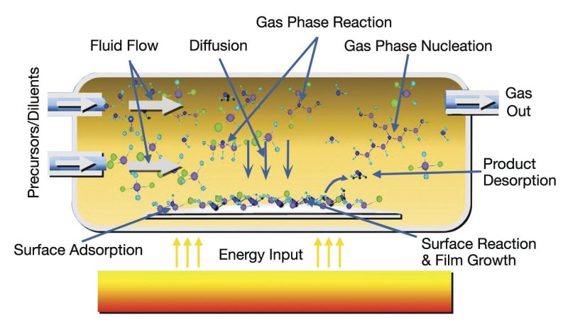
Figure 1. Aspects of a CVD process.
Figure 1 shows a schematic that can help in understanding the different processes in a CVD reactor. Chemical vapor deposition processes can be broken down into a number of discrete steps: First the precursor chemicals must be fed into the CVD reactor. Once in the reactor, precursor molecules must be transported to the substrate surface, usually through a combination of fluid transport and diffusion. Once on the surface, the precursor molecule must remain there long enough to react. After reaction occurs, the product thin film atom must remain on the surface while the by-product molecules must desorb from the substrate surface to make room for more incoming precursor molecules.
For now, we will not consider the pressure of the reaction nor the kind of reactor configuration, since these can vary widely and are often process-specific. The main common characteristics among different types of CVD processes is that, in all cases, the reactions or critical aspects of the reactions are thermally driven, and this requires that energy be added to the process. This energy can be in the form of heat to the substrate, plasma energy to the reactants or a combination of both.
The precursors used for CVD reactions must be of extremely high purity since any impurity will end up incorporated into the deposited film. Such impurities introduce uncontrolled changes in the material properties of the films that are detrimental to device performance. As a corollary to the statement on purity, CVD precursors must also be stable under storage conditions since any decomposition produces impurities that will be fed to the process. Ideally, CVD precursors only react under the temperature and pressure conditions that exist within the CVD process.
Precursors/Diluents
Typical precursors for CVD processes include:
- Oxygen
- Halides: H2SiCl2, HSiCl3, TiCl4, WF6, etc.
- Hydrides: SiH4, GeH4, AlH3(NMe3)2, NH3, etc.
- Organometallics: AlMe3, Ti(CH2tBu)4, etc.
- Metal Alkoxides: TEOS, Tetrakis Dimethylamino Titanium (TDMAT), Ti(OiPr)4, etc.
- Metal Dialkylamides: Ti(NMe2)4, etc.
- Metal Diketonates: Cu(acac)2
- Metal Carbonyls: Ni(CO)4
The first step in the actual CVD process is the controlled introduction of the precursors and any required diluent gases into the reaction chamber; this introduction is depicted on the left side of the chamber in Figure 1. To do this, the precursors must have sufficient vapor pressure to produce a stable, controllable flow to the process chamber. High pressure gases such as silane, hydrogen, ammonia, etc. meet this criterion and are easily delivered to the process using MFCs. Many liquids (e.g. halides such as dichloro- and trichlorosilane, titanium tetrachloride, tungsten hexafluoride, tantalum pentachloride; organometallic compounds such as TEOS, trimethylphosphate (TMP), aluminum alkyls, tetrakis(diethylamido) hafnium, tetrakis(dimethylamido)titanium, etc.) also have sufficient vapor pressure to produce stable, controllable flows using MFCs. Potential precursors having lower volatility, including volatile solids, present a problem for delivery to CVD reactors since most methods employed to date suffer from repeatability problems. In practice, a substrate is loaded into the process chamber and heated to the required process temperature under inert gas flow. Once the substrate is at temperature, the precursor/diluent gas mixture is introduced to the process chamber.
Fluid Flow/Diffusion
Once in the chamber, the precursor molecule is transported to the substrate surface by fluid flow effects, diffusion or a combination of both phenomena. These factors control the rate of arrival of precursor molecules at the substrate surface; this rate combined with the residence time/reactivity of the precursor on the surface, determines the rate of growth of the CVD film. In very low pressure CVD reactions (i.e., UHV-CVD), the precursor mean free path is of the same dimensional order as the size of the CVD process chamber and precursor molecules flow to the substrate surface without the interference of hydrodynamic boundary layer effects or gas phase reactions. Under these conditions, the rate of film growth is dependent only on the chemical reaction rate on the substrate surface provided that sufficient precursor is fed to the reactor inlet. Under intermediate pressures such as those in conventional LPCVD and PECVD processes (0.1 - 10 Torr), gas phase collisions and boundary layer effects more strongly influence precursor delivery to the substrate surface. LPCVD processes, while they are still primarily rate-limited by surface reaction rates, can be affected by mass transfer rates (diffusion rate) of precursor through the boundary layer to the substrate surface. LPCVD process conditions are designed with the assumption that the rate of film growth will not be limited by the rate of diffusion of precursor through the boundary layer rather than by the surface reaction rate, however, many LPCVD processes end up operating in a mixed regime where boundary layer effects play a role. The allowance for boundary layer effects plays a significant role in the physical configuration of most LPCVD reactors. A similar situation exists in PECVD reactors where mass transfer issues can influence the process even more strongly since the highly reactive chemical species produced in plasma result in much higher surface reaction rates. Additionally, LPCVD and PECVD reactors must be designed with care for surface-to-volume ratios and gas phase recirculation cells to avoid gas phase nucleation and particle contamination. APCVD processes operate at pressures of 760 Torr and, under these conditions, gas phase collisions and surface boundary layer effects dominate. Fluid flow patterns must be carefully managed within APCVD reactors to ensure that equal concentrations of reactants reach all parts of the substrate surface. As with LPCVD/PECVD processes, surface-to-volume ratios and gas recirculation zones are present and, in fact, are an even more critically important consideration for APCVD reactor designs.
Gas Phase Reaction and Nucleation
Depending on the chemical nature of the precursor as well as the temperature and pressure conditions within a CVD process, gas phase reactions may occur. All CVD reactors and processes are specifically designed to minimize or eliminate such reactions since they can lead to the nucleation of particulates in the gas phase and this can drastically reduce device yield. The reader should be aware, however, that some processes such as TEOS/ozone SACVD actually depend on the gas phase formation of reactive intermediate compounds in order to achieve beneficial process and product characteristics. This issue is highly process-specific and it is beyond the intended scope of this discussion.
Surface Adsorption and Reaction
While it may not be the controlling factor for growth rate in all forms of CVD, the adsorption and reaction of the precursor(s) on the substrate surface are obvious pre-requisites for thin film growth and it is worthwhile to take a moment to understand the processes that occur on the surface during thin film deposition. The factors that control the surface reaction are:
-
Precursor flux to the surface
- Controlled by fluid flow and/or diffusion (see above)
-
Availability of surface sites that will adsorb precursor molecules and retain them long enough for reaction to occur
- Controlled by product desorption rate and affected by adsorbed impurities
-
Substrate surface temperature
- Affects both residence time and reactivity of the precursor molecule
Once the precursor reaches the surface, it must adsorb and remain there long enough to react either by decomposition or with a co-reactant similarly adsorbed on the surface. The concentration of adsorbed precursors on a substrate surface is governed by the rate of arrival of precursor molecules at the surface; the proportion of incident molecules that stay on the surface; and the density of sites available for the adsorption of precursor molecules. Precursor arrival rates are also called the precursor flux and the probability of an incident molecule actually sticking to the surface once it arrives there is known as the "sticking coefficient". The rate of adsorption of precursor molecules is directly proportional to both factors and to the density of free adsorption sites on the surface. If reaction by-products remained adsorbed, they would block fresh precursor from adsorbing and thus slow the rate. Similarly, if impurities are present they may occupy surface sites limiting the adsorption of fresh precursor and slowing film growth rates.
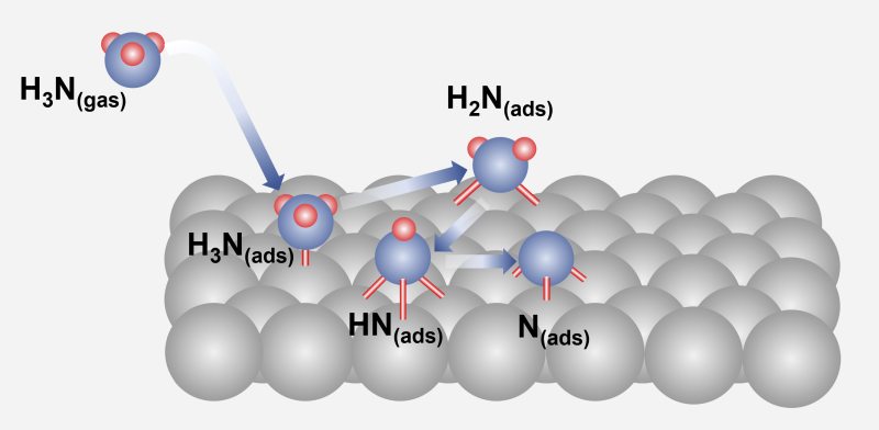
Figure 2. Decomposition of ammonia on a FCC metal surface.
Molecular precursors, once adsorbed on the substrate surface, undergo decomposition and/or reactions that are promoted by their interaction with the surface. A typical surface decomposition is represented by the adsorption and decomposition of ammonia, NH3, on a metal surface, shown in Figure 2. In this case, the ammonia molecule undergoes a step-wise decomposition to produce a nitrogen atom on the surface and hydrogen molecules which desorb into the gas phase. The hydrogen desorption rate is dependent on the temperature and the process pressure. As noted above, this rate impacts the overall rate of the deposition process since the sites occupied by hydrogen or other by-product atoms cannot adsorb incoming precursor molecules. Silane and other molecular precursors used in semiconductor CVD adsorb and decompose on silicon and other surfaces in an analogous manner.
The elemental adatoms (atoms that are adsorbed on a surface) that are created in the surface reactions are not stationary; in the case of a single crystal substrate such as a silicon wafer, they migrate across the surface until they encounter a high-energy surface site. High energy sites on a single crystal surface are sites such as atomic vacancies in a crystal face, lattice edges where a crystal plane ends and sites where a lattice edge experiences a "kink" (Figure 3).
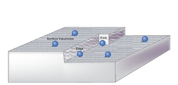
Figure 3. Vacancy, edge and kink sites on a substrate surface.
On non-crystalline surfaces such as silicon dioxide these well-defined high energy sites are not present, however, other types of surface sites act to trap adatoms. Once it encounters such a site, the adatom tends to remain stationary and to act as a starting point for surface nucleation of the desired thin film (Figure 4).
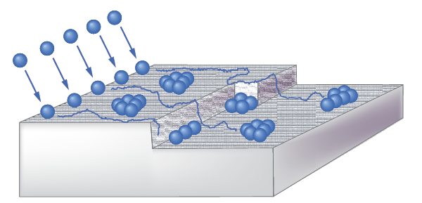
Figure 4. Adatom surface migration and nucleation.
Nuclei grow on the surface by the addition of migrating adatoms until they finally coalesce into a coherent film layer and the process begins again on this layer (obviously, this is an idealized view and actual growth will be "messier" with growth occuring over multiple layers and levels on a real surface). Figure 5 shows a highly-idealized picture of the different stages of film growth that follow the adsorption of atomic precursors on a substrate surface. These stages occur in all CVD and PVD thin film deposition processes.
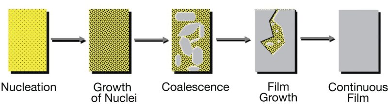
Figure 5. The stages of thin film growth.
Energy
The surface reactions that produce the thin films in these deposition processes require energy to promote the chemical reaction and to enable the surface migration of adatoms which produces nucleation and continuous film formation. In most deposition processes, thermal energy fulfills either all or a portion of the energy requirements of the process. Usually, this thermal energy is supplied using conventional resistive heaters, inductive heating or infrared lamps; the choice usually depends on the device requirements/limitations and the equipment configuration in use. Energy can also be supplied to the system in the form of high energy chemical species produced using a plasma. The plasma source is usually either a radio frequency (RF) or microwave power supply. Historically, plasmas that supplied reactive chemicals for the deposition have been created adjacent to substrate surfaces; however, many modern processes employ remote plasma sources from which the reactive species can be extracted and fed to the thin film process without incurring direct exposure of the substrate to the plasma. The reason for this lies in the fact that the free ions and electrons in a plasma can bombard the growing film, producing defects and adding impurities that are detrimental to its material properties.
Transport of Product Gases
In order for the chemical reactions that produce the thin films on the substrate surface to proceed at an acceptable rate, it is necessary to remove the product gasses from the deposition environment. This is usually accomplished using mechanical vacuum pumps or blowers. Obviously, pumping speeds, gas handling capacity and materials compatibilities of the pumping system must be matched to the inlet flows, reaction characteristics and physical/chemical properties of the product gases.
Related Topics
Thin Films
- Polycrystalline Silicon Thin Films
- Silicon Based Epitaxial Thin Films
- Compund Semiconductor Epitaxial Thin Films
- Dielectric Thin Films
- Metal Thin Films
Thin Film Deposition
For additional insights into semiconductor topics like this, download our free MKS Instruments Handbook: Semiconductor Devices & Process Technology
Request a Handbook Ultra-High Velocity