Wafer Surface Cleaning
The increase in etch and deposition steps, new materials, and new structures used in 2.5D and 3D packaging rely heavily on cleaning processes like photoresist strip and descum to ensure contamination free surfaces. Devices require varying levels of cleanliness using different materials throughout the manufacturing process so it is increasingly important to offer multiple cleaning options to achieve the required clean levels to ensure good devices and high yield. Surface activation, an important process tied to cleaning, conditions and prepares the surface for the next process step ensuring good quality adhesion resulting in high quality die.
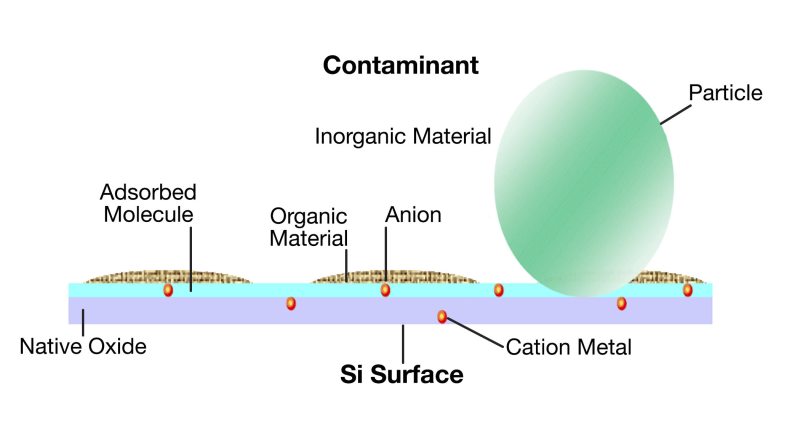
Figure 1. The surface contaminants that may be present on a silicon wafer.
Prior to a wafer's entry into the fabrication process, its surface must be cleaned to remove any adhering particles and organic/inorganic impurities. Silicon native oxide also needs to be removed. Continually shrinking device design rules have made cleaning technologies ever more important to achieving acceptable product yields. In modern device fabrication, wafer cleaning procedures can make up 30% - 40% of the steps in the total manufacturing process. Wafer cleaning has a long developmental history within the semiconductor industry. See collections and studies of the classic methods from authors such as Werner Kern, and Tadahiro Ohmi for more detailed discussion.
Contaminants on wafer surfaces may be present as adsorbed ions and elements, thin films, discrete particles, particulates (clusters of particles), and adsorbed gases. Figure 1 shows a schematic of the kinds of contaminants present on the wafer surface prior to it entering the process flow; Table 1 describes the impact of the different kinds of surface contamination on device performance while Table 2 shows the cleaning solutions employed to remove the different contaminants.
| Type of Contamination | Main Influences on Device Characteristics | |
|---|---|---|
| Particle Contamination |
|
|
| Metallic Contamination | Alkali Metals |
|
| Heavy Metals |
|
|
| Chemical Contamination | Organic Material |
|
| Inorganic Dopants (B, P) |
|
|
| Inorganic Bases (amines, ammonia) & Acids (SOx) |
|
|
| Native and Chemical Oxide Films Due to Moisture, Air |
|
|
Table 1. Wafer contamination and its effects.
| Contaminant | Cleaning Procedure Name | Chemical Mixture Description | Chemicals |
|---|---|---|---|
| Particles | Piranha (SPM) | Sulfuric acid/hydrogen peroxide/DI water | H2SO4/H2O2/H2O 3-4:1; 90°C |
| SC-1 (APM) | Ammonium hydroxide/hydrogen peroxide/DI water | NH4OH/H2O2/H2O 1:4:20; 80°C | |
| Metals (not copper) | SC-2 (HPM) | Hydrochloric acid/hydrogen peroxide/DI water | HCl/H2O2/H2O1:1:6; 85°C |
| Piranha (SPM) | Sulfuric acid/hydrogen peroxide/DI water | H2SO4/H2O2/H2O3-4:1; 90°C | |
| DHF | Dilute hydrofluoric acid/DI water (will not remove copper) | HF/H2O1:50 | |
| Organics | Piranha (SPM) | Sulfuric acid/hydrogen peroxide/DI water | H2SO4/H2O2/H2O 3-4:1; 90°C |
| SC-1 (APM) | Ammonium hydroxide/hydrogen peroxide/DI water | NH4OH/H2O2/H2O 1:4:20; 80°C | |
| DIO3 | Ozone in de-ionized water | O3/H2O Optimized Mixtures | |
| Native Oxide | DHF | Dilute hydrofluoric acid/DI water | HF/H2O 1:100 |
| BHF | Buffered hydrofluoric acid | NH4F/HF/H2O |
Table 2. Cleaning solutions used to prepare substrates for the CMOS process.
Particle Contamination
Particle contamination can originate as airborne dust from a variety of sources including fab equipment, process chemicals, the internal surfaces of gas lines, wafer handling, gas phase nucleation in film deposition systems, and fab operators. Even particles of low nanometer dimension have the potential to generate "killer" defects, either through the action of physically occluding the formation of key features in the device (producing patterning, feature and implant defects) or by creating localized electrically weak spots in thin insulating films. Cleaning solutions for particle contamination include piranha cleans for gross particulate (and organic) contamination and SC-1 cleans for small, strongly adhering particles. Piranha solutions are extremely strong acids which oxidize many surface contaminants to produce soluble species that can be removed in solution. SC-1 solutions remove insoluble particles by oxidizing a thin layer of silicon on the surface of the substrate which then dissolves into the solution, carrying adsorbed particles with it. Modern SC-1 cleans employ megasonic (0.8 - 2.0 MHz) vibration to aid in the removal of particles from the surface. SC-1 solutions prevent re-adsorption of the particle by inducing the same zeta potentials a measure of electrostatic repulsion, on the particle and substrate surfaces. All cleaning solutions that contain hydrogen peroxide (piranha, SC-1, SC-2) leave a thin oxide layer on the silicon wafer surface.
Metal Contamination
Semiconductor devices are particularly sensitive to metallic contaminants since metals are highly mobile in the silicon lattice (especially metals such as gold) and therefore they easily migrate from the surface into the bulk of the silicon wafer. Once in the bulk silicon, even moderate process temperatures cause metals to rapidly diffuse through the crystal lattice until they are immobilized at crystal defect sites. Such "decorated" crystal defects degrade device performance, permitting larger leakage currents and producing lower breakdown voltages. Metal contaminants can be removed from the substrate surface using an acidic clean such as SC-2, piranha or dilute hydrofluoric acid (HF); these cleans react with the metal to produce soluble, ionized metallic salts that can be rinsed away.
Chemical Contamination
Chemical contamination of the substrate surface can be broken down into three types: surface adsorption of organic molecular compounds; surface adsorption of inorganic molecular compounds; and an ill-defined, covalently-bound thin (ca. 2 nm) native oxide consisting of the chemical oxide/hydroxides of silicon, SiOx(OH)y.
Organic Compounds
Surface contamination by organic compounds either through airborne contamination or as residue from organic photoresists (PRs) is omnipresent in cleanrooms due to the presence of volatile organic solvents/cleaners and outgassing from polymer construction materials. Gross contamination by organics, such as occurs with incomplete PR removal, can impact device yields by leaving residues that form carbon during high temperature process steps. These carbon residues can form nuclei which behave as particle contaminants. Small amounts of residual metal resident in the PR compound can be trapped on the surface in these carbon residues]. PR residual contamination can be removed using piranha cleans and other high efficiency PR cleanup methods, as described in Dry Substrate Surface Cleaning.
Organic contamination due to ubiquitous volatile airborne contaminants also require removal from the wafer surface. The presence of these contaminants can hinder the removal of native oxide by dilute HF solutions (see below), producing poorly defined interfaces between the gate oxide and the substrate and gate electrode. Poor interface characteristics strongly degrade gate oxide integrity. The presence of organic compounds on the surface can affect the initial rates of both thermal oxidation and CVD processes, introducing undesirable and unknown variations in film thickness. The SC-1 clean removes these organic residues through oxidation by peroxide and solvation of the products by NH4OH. The SC-1 clean slowly removes any native oxide, replacing that layer with a new oxide produced by the oxidizing action of the peroxide. In recent years, ozone dissolved in DI water (DIO3) is finding increasing use as a replacement for older Pirhana and SC-1 cleans as a "green" and safer alternative for the removal of organic contaminants.
Inorganic Compounds
Chemical compounds containing dopant atoms such as boron and phosphorus can be present on wafer surfaces due to effects such as the outgassing of phosphorus-containing flame retardants or dopant residuals in process tools. If they are not removed from the wafer surface prior to high temperature processing, these elements can migrate into the substrate, modifying the targeted resistivity. Other kinds of volatile inorganic compounds such as basic compounds like amines and ammonia and acidic compounds like sulfur oxides (SOx) will also produce defects in semiconductor devices if they are present on the substrate surface. Acids and bases can cause unintentional shifts in the basicity or acidity of chemically amplified resists leading to problems in pattern generation and resist removal. These compounds are highly reactive and will readily combine with other volatile ambient chemical species to create particles and haze due to the formation of chemical salts on the substrate surface. Adsorbed acidic and basic species can be removed from the substrate surface by the combined action of SC-1 and SC-2 cleans.
Native Oxide
Silicon, like many elemental solids, naturally forms a thin layer of oxidized material on its surface by reaction with oxygen and moisture in the ambient air. The chemical formulation of this layer is not well-defined, being a more or less random aggregation of Si-O-Si, Si-H and Si-OH species. The presence of this native oxide on the silicon surface causes problems in semiconductor device manufacturing since it can lead to difficulties in controlling the formation of very thin thermal oxide thicknesses. Any native oxide that is present on the substrate during thin gate oxide formation will electrically weaken the gate insulator through the incorporation of hydroxyl groups. Additionally, if native oxide is present on the silicon surface of a contact pad, it will increase the electrical resistance of that contact. Over the past 50 years, our understanding of the nature of silicon native oxide and its impact on device performance has greatly increased. These studies found that very dilute solutions of HF, in de-ionized water, DI, or dilute solutions of ammonium fluoride, NH4F, HF and DI water (buffered oxide etch, BOE) completely remove silicon native oxide, leaving a hydrogen-terminated clean silicon surface according to Figure 2.
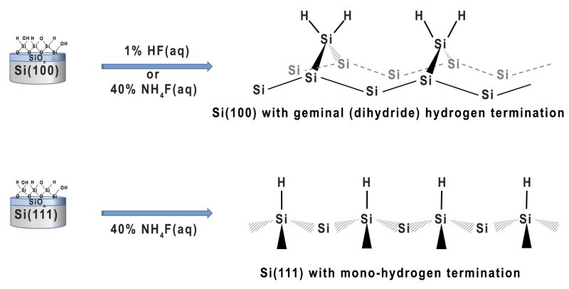
Figure 2. Native oxide removal and H-terminated silicon surface characteristics.
RCA Cleaning
The first successful wet-cleaning process for front-end-of-line (FEOL) silicon wafers was developed at RCA by Werner Kern and co-workers and published in 1970. Since then, there have been many developments and successful modifications of the approach and RCA cleaning continues to be the primary FEOL pre-deposition cleaning in the industry today.
RCA cleaning procedures are a combination of the different procedures described above. The process consists of consecutive SC-1 and SC-2 solutions, followed by treatment with a dilute HF solution or buffered oxide etch (BOE). The product is a clean, hydrogen-terminated silicon surface, ready to be used in the process flow.
Wafer Surface Cleaning Products


Related Topics
Wafer Cleaning
Front-end Semiconductor
For additional insights into semiconductor topics like this, download our free MKS Instruments Handbook: Semiconductor Devices & Process Technology
Request a Handbook Ultra-High Velocity